Download
1 / 30
340 likes | 590 Vues
A Monolithic Low-Bandwidth Jitter-Cleaning PLL with Hitless Switching for SONET/SDH Clock Generation. D. Wei, Y. Huang, B. Garlepp and J. Hein Silicon Laboratories Inc., Austin, Texas Presented in ISSCC, Feb, 2006. New Breed of Analog Designers: digAnalog .

E N D
A Monolithic Low-Bandwidth Jitter-Cleaning PLL with Hitless Switching for SONET/SDH Clock Generation D. Wei, Y. Huang,B. Garlepp and J. Hein Silicon Laboratories Inc., Austin, Texas Presented in ISSCC, Feb, 2006
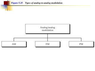
New Breed of Analog Designers: digAnalog • Requirement for analog interface is higher and higher (i.e. multimedia application), yet technology advancement shies away from the analog performance • Example: 1/f noise, gate leakage, device non-ideality • Digital signal processing is so powerful today! • Deep sub-micron CMOS • More computation power for limited-size area • Integration is the trend • Consumer electronics require compactness • Delicate process means higher ASP and lower revenues Q: can we enhance the “analog” performance by the power of “digital”?
Insights of Analog-to-digital Interface Go against the technology trend
Insights of Analog-to-digital Interface (con’t) Demand faster technology but with less accuracy!
digAnalog Design Rules • Good understanding of the system requirements • “To dig or not to dig, that is the question” • Pick the right “candidate” (voltage, current, flux, phase, …) to process • What defines your “signal”? • Faster technology available (and cheap!) • signal bandwidth vs. sampling clock
SONET/SDH Clock Management • 100% Redundancy is required at the line-card timing reference
Type-II PLL Phase Transient During Reference-switching • Dmax : maximum phase deviation • d/dt : maximum phase step slope
Maximum Time Interval Error (MTIE) Phase Offset (25.7ns max) slope < 81ns/1.326ms Frequency Offset (9.2ppm max) • Typical LBW choice: 250Hz (clk rearrangement) ~ 1KHz( frequency translation)
“Hitless” Phase-Switching Architecture t=t1, selA=1 / selB=0 fA- foffsetA,0 = fout,1, foffsetB,1 = fB t=t2, selA=0 / selB=1 fB- foffsetB,1 = fout,2, foffsetA,2 = fA Dfout,1,2 = (fA-fB)-(foffsetA,0-foffsetB,1) = 0 if fA and fB ~ constant
Digital Implementation of Hitless Switching (1) • PLL LBW < 12KHz • PFD SDADC fs = 311MHz
“shift” the offset DAC value • AZ bandwidth ~ 100KHz • D avoids the DAC overflow PFD ADC and Auto-zero Loop • Loop Bandwidth < 12KHz vs. SDADC fs = 311MHz SNR > 22bits • PFD full scale = 6.42ns Offset DAC LSB ~ 100ps
What if Frequency Error Is Present? Dfoffset,max =FSPD <8FSPD modulus (k=0~7) Dfout,1,2 = (fA-fB) - (foffsetA-foffsetB) – k (0.5 2FSPD) • 2FSPD: Phase Detector Full-scale (6.42ns)
Digital Implementation of Hitless Switching (2) • Each swallow: TD = 8Tvco
Phase Transient Measurement Setup adjustable Df • Linear phase detector “demodulates” the DUT output phase • LOS (loss-of-signal) on clkB triggers the oscilloscope
Measured Phase Transient During Reference-switching Wandering due to LOS Loop relocks the phase 116ps PD out residual Df = 35ps LOSB trigger the switching • Initial Df = 180 (~25ns) LOSB • Mode: Auto-switching (LOS triggers the switching)
Removing the External Loop Filter • DSP implementation replaces the bulky external loop filters (LF) • Less Bill-of-Materials (BOM) • Avoid excess noise-coupling at post-LF nodes
Gain ratio controls LBW and peaking DSP-based Loop Filter Implementation • No external loop filter components needed
For Type-II PLL with low-peaking (d<0.1dB), KF ~ LBW / (KPD x Kv) KI ~ (LBW)2 x (d-1) / (KPD x Kv) Input bits accumulated feedforward bits added varactor codes Reduced by SD (rounding) PLL Bandwidth and Peaking Control Feedforward (F) PFD ADC Integration (I)
2nd-order SD generates varactor cntl. voltage DAC expander reduces the analog hardware cost by 16x Connecting the Loop Filter to Varactors
Varactor DAC and Multiplexer • At any instant, only 8 varactors receive DAC tuning voltages
DAC Movement Across Sub-Varactor • Accumulator bits slowly move the DAC banks • Feedforward bits vary the tuning voltage Vg
Chip Micrograph reference generator. output drivers PFD/ADC B VCO divider 3.5mm digital routes / regulators PFD/ADC F varactor master regulator PFD/ADC A DAC expander multiplexer 5.1mm
discrete solution hybrid solution 23mm 50mm 23mm 50mm 11mm 11mm presented solution Discrete Solution vs. Integrated Solution • No external loop filters are required. • dramatically simplifies the line card design!
Jitter Generation Jitter Transfer -20 2 Phase Noise @ LBW=800Hz 622.08MHz Output 0 -40 -2 -60 -4 6400Hz -80 -6 3200Hz L(f) (dBc/Hz) -97dBc/Hz @10KHz Loop Transfer (dB) -8 -100 1600Hz -10 800Hz -120 -12 19.44Mhz Input 622.08MHz Output -142dBc/Hz @1MHz -140 -14 -160 -16 100 1K 10K 10 100 1K 10K 100K 1M 10M 100M Frequency (Hz) Frequency (Hz) PLL Characteristics Measurement • Measured integrated jitter: • OC48 band 0.69ps • OC192 band 0.26ps • Measured peaking: < 0.1dB
Conclusion • Digital “hitless” clock-switching is demonstrated, enabling the on-chip implementation for SONET/SDH clock management. • Loop components are digitally implemented, which minimizes the external noise coupling and also has the good control over loop characteristics. • Concise digital implementation of digital varactors simplifies the hardware implementation, and enhances the VCO performance, enabling the “jitter-cleaning” to the PLL input clocks.