Download
1 / 20
360 likes | 986 Vues
CMOS Image Sensor. Daniel Aguirre Utah State University Mechatronics MAE/ECE5320. CMOS Image Sensor. CMOS- Complimentary Metal Oxide Semiconductor Primary uses: Digital Cameras Digital Camcorders Cellular Phones Security Cameras Surveillance application

E N D
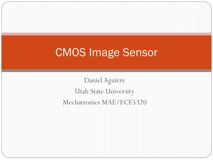
CMOS Image Sensor Daniel Aguirre Utah State University Mechatronics MAE/ECE5320
CMOS Image Sensor • CMOS- Complimentary Metal Oxide Semiconductor • Primary uses: • Digital Cameras • Digital Camcorders • Cellular Phones • Security Cameras • Surveillance application • Also used in a large number of industrial, medical, media, and consumer applications.
APS (Active Pixel Sensor) A CMOS image sensor is an APS that uses a CMOS process. An APS is an integrated circuit that contains an array of pixels each containing a photo detector and system to amplify the signal from the photo detector. CMOS image sensor (ref 1)
What is a pixel? In simple terms a pixel is a dot. A digital picture is made up of many, often millions of the these dots. The resolution of the these pictures depend on; the size of pixels, the distance between pixels, and the number of pixels that comprise the image.
Large vs. Small Pixels The image on the right has small pixels where the image on the left has larger pixels or it can also be explained that the image on the right has a higher number of pixels per area than the image on the left.2
What is a CMOS Process? “Complementary” Use of complementary and symmetric pairs or p-type (increased number of free charge carriers) and n-type (containing extra conduction electrons) metal oxide semiconductor field effect transistors for logic functions.3 “Metal-Oxide-Semiconductor” References to the physical structure of certain field effect transistors, having a metal gate electrode placed on top of an oxide insulator, which is on top of a semiconductor material.3
How does it work? An array of light sensitive diodes collect light, kind of like a solar cell, and emit a signal. That signal is amplified and send to a decoder that resolves the signal into a dot. And a computer program places the dot in it’s respective place from the array into the image. Array set-up for CMOS sensor4
Image Taking Structure • Array of pixels, each containing a photodiode to convert photons into electrons and transistors to generate voltage. • Each pixel is controlled by a reset switch, which clears the device of all charge prior to the next exposure. • At the time of capture, the pixel is charged by the light. This charge is then converted to a voltage at the pixel level. • The voltage signal then passes through the automatic gain controller (AGC) and analog-to-digital converter (ADC) before leaving the CMOS chip.
Color Color is determined much like a printer. • Three colors are used either Red,Blue, and Green scheme or Magenta, Cyan, Yellow scheme. Determined by either additive coloration or subtractive coloration respectively. • As the pixels get smaller the three color scheme blends the three colors into a color that matches the color that was seen by the one taking the picture. As seen in slide 5
Pixels and Color Each pixel is covered further with an array of light filters allowing only certain colors of light through. The light that is passed through hits a sensor that sends the signal to tell the processor that this color is at this dot. Ref. 6
2 Methods of Light Gathering • Front-illuminated structure • Back-illuminated structure 7
Front-illuminatedstructure In front-illuminated structure sensors the actual light collecting system is semi-buried deep in the structure of the silicone wafer. Even though light can reach the diodes and light is gathered fairly abundantly, the light is obstructed through the thickness of the wafer. The reason this is done is because it easier to place the diodes at the bottom of the wafer and it gives the light receiving surface protection.
Back-illuminatedstructure Back illuminated structure places the photodiodes and light receiving surface above the wiring and on top the wafer. This method, though slightly more expensive and extensive to assemble, allows more true light to get to the light receiving surface and into to photodiode. Creating a more true to real color coming through the lenses because there is less obstruction.
CCD (Charge Coupling Device) The major competitor in the digital image sensors is the CCD sensor • Though both sensors were theorized and developed at the same time, CCD technology received the most momentum from the start: • Due to ease of construction and available materials • At the beginning CMOS sensors were expensive and yeilded very poor imaging • Since CMOS sensors have been further developed: • Yielding higher resolution images because of decreased wafer thickness and pixel size available to put on wafer • Generally consume less power • Single voltage power supply (reducing the number of amplifiers required. Ref 8
Consumer Products or Industry • You can find CCDs in low-cost low-power cellphone cameras and CMOS sensors in high-performance professional and industrial cameras • CCD sensors can be produced quickly and inexpensively but quality and pixel size, like one would think, are sacrificed with cost • CMOS sensors, although initially thought to be less expensive because the chip has similar make-up as the mainstream memory wafer, have become very extensive in fabrication processes and material sciences. • However, both are found abundant in both arenas and are subject to performance and cost relativity.
Characteristics of a typical CMOS sensor CMOS Sensors – Typical Characteristics • Zero or First Order System depending on how photodiode capacitance is used. • Power Consumption – 200 mW • Dynamic Range – 70+ dB (Human DR is ~90dB) • Spectral Range – 200nm to 1100nm with 700nm peak. • Response time can be as little a 1ms. • Fixed Pattern Noise - ~16% p-p • Fill Space – 30-40% of each pixel can be used to capture light. • Automatic Gain Control – driven by feedback from other optical components, and image processing algorithms. • Generally low SNR due to various noise sources • Low Power Consumption • Additional Digital Logic Capability Ref 9
Electrical noise always exists and will affect whatever sensor you are using • Noise Sources • Temporal Noise – random noise often caused by the random arrival of photons onto the sensor. Similar noise can be induced by the random arrival of electrons to an electrical element of the sensor. This includes arrival of pixel voltages to column amplifiers, AGCs and ADCs. • Amplifier Noise – Thermal noise is generated by uncorrelated sampling operations. • Analog-Digital Conversion – Inherent noise in quantization of analog signal. • Fixed Pattern Noise – Spatial noise due to mismatches in pixels or CFAs. This can also be caused by variations in various amplifiers or converters Ref 9
CMOS Sensor Price Examples Cypress 6.6 MP APS: $377 Used for machine vision, biometry and document scanning. Cypress Aptina 5MP APS: $33 Used for digital video cameras and still cameras Omnivision 5MP APS: $15 Used for mobile phones, PC multimedia, toys, and digital still cameras Ref 9
References • Wikipedia: http://en.wikipedia.org/wiki/CMOS_sensor • http://mashable.com/2012/01/20/pixel-art/ • Wikipedia: http://en.wikipedia.org/wiki/CMOS • http://www.siliconimaging.com/ARTICLES/CMOS%20PRIMER.htm • http://www.moglik.com/i/show/4255/camera-sensor-cmos-diagrama.htm • http://www.sensorcleaning.com/whatisasensor.php • http://www.i-micronews.com/lectureArticle.asp?id=1607 • http://micro.magnet.fsu.edu/primer/digitalimaging/cmosimagesensors.html • http://mech207.engr.scu.edu/SensorPresentations/Patel%20-%20CMOSImageSensor%20Combined.pdf