Download
1 / 87
890 likes | 1.44k Vues
68HC11 Parallel I/O. Chapter 7. Microcontroller-Based System. To I/O. CPU: Central Processor Unit I/O: Input/Output Memory: Program and Data Bus: Address signals, Control signals, and Data signals. Microcontroller e.g. M68HC11. Terminology.

E N D
68HC11 Parallel I/O Chapter 7
Microcontroller-Based System To I/O CPU: Central Processor Unit I/O: Input/Output Memory: Program and Data Bus: Address signals, Control signals, and Data signals Microcontroller e.g. M68HC11
Terminology • Pin – This is a physical point that connects the microcontroller to the outside world. • I/O – Input /Output • Input – This is an input pin • Output – This is an output pin • Bidirectional I/O – This is pin which can be configured as either input or output. • Port I/O register= This is a data registerthat is physically connected to a set of I/O pins • Control register = This a control register used to configure the operation of a data port or some other function on the controller.
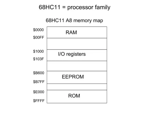
Terminology • Memory-mapped I/O: Microcontroller configuration in which external I/O is accessed using normal memory access instructions. • The M68HC11 uses memory mapped I/O. • This is in contrast to other microprocessors (e.g. Intel) which have a separate I/O address space and use special instructions to access it.
Input Buffer Din Equation Symbol Input pin Truth Table
Output Buffer Dout Equation Output pin Symbol Truth Table
Another meaning of “buffer” • The word buffer is also frequently used in computer engineering to refer to a region of storage (registers or memory) that is used to hold data temporarily while it is being (or waiting to be) sent or received. • This usage is contrasted with an electrical buffer (previous slides) which just amplifies and delays a signal.
Multiple Outputs Y lower A A Y Y 0 1 raise Chip B Chip A Let A_A = 0 Let B_A = 1 What is Y? Unknown X
Tri-State Driver Active-low signal “OEn”(Output Enable) Equation Symbol Truth Table High Impedance State “Open Circuit”
One implementation Of a tristate buffer in CMOS… Vdd Output-drivinginverter CMOSTransmissionGate A A Y OEn GND
Multiple Outputs Y Bus Driver Floating 0 1 raise Chip A Chip B Let A_A=1 Let B_A=0 Y=1 1 0 controller
Multiple Outputs Y Bus Driver Floating 0 1 Chip B Chip A Let A_A=0 Let B_A=1 Y=0 0 1 controller
Field Effect Transistors - FETS A FET acts like a “switch” If Vgate is ONE, switch is closed, connecting A and B otherwise A and B are isolated. B Field Effect Transistor (FET)
Open Drain Output Driver We can use an FET as an Output Driver When Din=1, Dout=0 When Din=0, Dout=Z “open circuit” How does Dout become an ONE?
Open Drain Output Driver Use an external pull-up resistor When Din=1, Dout=0 FET is ON, Dout=0 When Din=0, Dout=1 FET is OFF, Dout is pulled up to VDD Why do this?
Simple Data I/O Control Controller sends data to Chip-A and Chip-B Halt B A Data However, either device can “Halt” the transfer by bringing the halt line low. “Wired-OR” configuration
Bi-directional I/O Driver • Allows a single pin to be configured as an input buffer or an output buffer.
Bi-Directional I/O Buffer Symbol Tri-state Buffer Function Table From Ckt dio Pin ToCkt Input Buffer Note: I/O buffer is either Input or output
Bi-Directional I/O Bufferas Input Buffer Symbol 1 Floating Dio (Input) To_ckt Input Buffer To_ckt = Dio
Bi-Directional I/O Bufferas Output Buffer Symbol 0 Active Dio is From_ckt From_ckt Dio (Output) To_ckt Note: To_ckt is also From_ckt Input Buffer
68HC11 Parallel I/O Ports Section 7.4
M68HC11 Port Summary • PortA • 1 bidirectional, 3 input, and 4 output port • Timer port • PortB • 8-bit fixed output port • Used for high byte of mem. addr. in expanded mode • PortC • 8-bit bidirectional parallel port • Used for low byte of address & for data in expanded mode • PortD • 6-bit bidirectional parallel or serial I/O port • PortE • 8-bit digital or analog input port One of the 4 outputs isbidirectional on the E9
M68HC11E block diagram From datasheet, p.17
Tangent on Operating Modes • The HC11 has four operating modes. • These are selected by input signals on the MODB and MODA inputs when the chip is reset. (from HC11 Reference Manual, p.47)
Default Memory Maps of HC11E9 (From the HC11E series datasheet, p.37)
Ports B and C are mode-dependent Reference manual, p. 62
Example pin connections in single-chip HC11 systems • Very simple configuration. • A small amount of external circuitry is still needed, for: • Power supply conditioning • External clocking • Low-voltage reset • Setting mode bits • Note there is no external ROM/RAM in this mode! • But B and C ports are available for doing parallel I/O. (Reference manual, p.117)
Demultiplexing address/datain Expanded modes Datasheet, p. 34
Connecting External memory Reference Manual, pp. 117-118 PC PB
Connecting External Memory • Note in this example, the 8K EPROM Chip is Selected (CS) if A13 & A15 are high. • And, A0-A12 are fed to the EPROM. • Therefore, what range(s) of addresses does the EPROM chip map to? Reference Manual, p. 118
Port A – Address $1000 • An 8-bit, parallel I/O port. • Data address $1000 (normally) • Multi-Function • I/O Port • Timer Port • PACTL – Port A Control Register ($1026) • determines port function
Port A – I/O Pin Modes • Bits 0-2: Input Bits • PA0-PA2 • Bits 3-6: Output Bits • PA3-PA6 • Bit 7 Bidirectional Bit • Direction set in PACTL Except that PA3 isbidirectional in the E9
7 6 5 4 3 2 1 0 Port A - $1000 Data B O O O O I I I Bits Notation: PA7 = Bit 7 of Port A PA6 = Bit 6 of Port A PA5 = Bit 5 of Port A ………………………………. PA0 = Bit 0 of Port A O=Output I =Input B=Bidirectional
Port A Circuit Schematic This one is also bidirectional in the HC11E’s
Port A – I/O Port Mode • Example: * Bit 7 configured as input (default) PortA EQU $1000 * Output a $C to Port A Outdata EQU %01101000 ;Sets bits 3,5,6 ………… * Output data to PortA LDAA #Outdata STAA PortA * Read Data from PortA LDAA PortA
DDRA7 PAEN PAMOD PEDGE 0 0 RTR1 RTR0 7 6 5 4 3 2 1 0 Bits PACTL: $1026Port A Control Register This is DDRA3 in the E series • DDRA7 = Data Direction Register A7 • 0 = Input Direction (Default) • 1 = Output Direction • PAEN = Pulse Accumulator System Enable • 0 = Disable (Default) • Port A is set for I/O function • 1 = Enable • Port A is set for Pulse Accumulator function • (part of timer system, to be discussed later)
LED Circuit Example Switch Light On Light Off
68HC11 LED Example • We’ll use PA7 for Input, PA6 for output • PA7=0 switch open, PA7=1 switch closed • PA6=0 LED off, PA6=1 LED on • Pseudo-code: • Configure PortA ; • Repeat • IF(PA7=0) then ; Switch is open • PA6=0 ; Turn LED OFF • Else • PA6=1 ; Turn LED ON • EndIF • Until Forever
Program, using BRSET/BSET/BCLR • These instructions allow us to manipulate individual bits, but they force us to use indexed addressing to refer to the I/O registers • Extended direct mode is not available with these particular instructions BIT6 EQU %01000000 ; Mask for bit 6 BIT7 EQU %10000000 ; Mask for bit 7 IOBASE EQU $1000 ; Base of I/O config registers PORTA EQU $00 ; Offset of PORTA ($1000) PACTL EQU $26 ; Offset of PACTL ($1026) start: LDX #IOBASE ; Point X at I/O config registers CLR PACTL,X ; Clear all PACTL control flags. loop: BRSET PORTA,X BIT7 on ; If port A bit 7 is set, turn LED on BCLR PORTA,X BIT6 ; else, turn LED off. (Clear bit 6) BRA endif ; Go to end of if statement. on: BSET PORTA,X BIT6 ; Turn LED on (set bit 6). endif: JMP loop ; Repeat.
Port B • 8-bit port • Fixed Direction: Output • Data address: $1004 • Writing to Address $1004 will write to the port. • Example: PortB EQU $1004 Value EQU $F2 ... LDAA #Value STAA PortB • When the HC11 is in expanded mode, on boards with no Port Replacement Unit, • Port B is reserved for the upper 8 address bits (AD9-AD15)
7 6 5 4 3 2 1 0 Port B - $1004 Data O O O O O O O O Bits O=Output
Port C • 8-bit bidirectional port • Data address: $1003 • Multi-Function: • In single-chip mode, or with a Port Replacement Unit • I/O Port • Latched data from Port C is available at address $1005 • It’s latched when a rising edge occurs on STRA pin • Handshaking port • In expanded mode with no Port Replacement Unit, • Used for low 8 bits (AD0-AD7) of memory address bus and for memory data bus (D0-D7) • PIOC – Parallel I/O Control Register C determines function
7 6 5 4 3 2 1 0 Port C - $1003 Data B B B B B B B B Bits O=Output I =Input B=Bidirectional
7 6 5 4 3 2 1 0 DDRC - $1007 DDCn= Data Direction Bit n DDC7 DDC6 DDC5 DDC4 DDC3 DDC2 DDC1 DDC0 Bits DDCn: 0 = Input (Default) 1 = Output
7 6 5 4 3 2 1 0 PORTCL - $1005 Latched Data B B B B B B B B Bits O=Output I =Input B=Bidirectional