Download
1 / 23
230 likes | 381 Vues
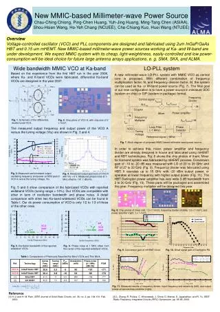
An X-Band Low Noise InP-HBT VCO with Separate Optimized Varactor Layers. T. Magrisso (1) D. Elad (1) N. Buadana (1) S. Kraus (2) D. Cohen Elias (2) A. Gavrilov (2) S. Cohen (2) D. Ritter (2). (1) RAFAEL, Armament Development Authority Ltd., Microelectronic Directorate

E N D
An X-Band Low Noise InP-HBT VCO with Separate Optimized Varactor Layers T. Magrisso (1) D. Elad (1) N. Buadana (1) S. Kraus (2) D. Cohen Elias (2) A. Gavrilov (2) S. Cohen (2) D. Ritter (2) (1) RAFAEL, Armament Development Authority Ltd., Microelectronic Directorate (2) Department of Electrical Engineering, Technion-Israel Institute of Technology
InP Based VCOs • Record frequencies • Optoelectronic integration: Optoelectronic Oscillitor, • Clock recovery, etc..
Previous work on InP HBT circuits at Technion: 43 GHz integrated TWA photoreceiver • 75 GHz TWA
Varactors in InP HBT VCOs • Previous InP HBT VCOs used base collector layers • as varactor layers. • Optimized HBT requires fully depleted collector • at Vbc=0, for minimum VCO’s phase noise. • As a results, small tuning range is obtained
10um 1um Conventional InP HBT technology P N N+ InP N+ Emitter N P N Ga InAs P Base Ga InAs N Collector N+ Ga InAs N+ Sub-Collector InP Semi-insulating Substrate
Separate varactor layers • Varactors and HBTs can be separately optimized. • Varactor layers can be grown either above or underneath • the transistor layers. • Varactor layers underneath transistor layers • complicate interconnect. • Varactor layers above transistor layers • require stepper technology.
InP HBT technology with Separate Varactor Layers N P N InP N+ Emitter Ga InAs P Base InP N Collector N+ InP N+ Sub-Collector P N Ga InAs P Base InP N Varactor N N+ InP N+ Varactor Connect InP Semi-insulating Substrate
This Work • Carried out by contact lithography-varactor layers • underneath transistor layers. • Wide tuning range Colpitts X band VCO demonstrated • as first attempt. • Simplified VBIC transistor model predicts well • VCO’s performance.
Transistor Properties • Ft=180 GHz • Fmax=200GHz • Vturn-on=0.5V • Vce-breakdown=5V • Ic max (Vce=3v)=30mA • βAC=50
Transistor Modeling • DC Measurements and s-parameters • Small-signal equivalent circuit parameters extraction. • Degenerate VBIC model with 18 parameters only
VBIC model parameters extracted at specific bias, Does it work for large signal VCO modeling ?
Varactor Design & Modeling We have compared 2 types of varactors: • Base-Collector layers. • Separate layers with Nd=1017 cm-3.
Varactor Modeling • Different size varactors, for scaleable model extraction. • Semi-lumped model • Rectangular varactors achieving 1 ohm series resistance.
Varactor modeling Using simple model with text book equations.
Comparison between Measurement and Simulation with degenerate VBIC model
Phase Noise Simulation Phase noise parameters extraction for VBIC model Kfn=1E-12 Afn=1
Conclusions • InP HBT X band VCO with separate varactor layers • underneath transistor layers achieved tuning range of • 12% and phase noise of -94dB/Hz at 100KHz. • Future work: VCO layers on top of transistor layers for • higher frequencies, and optoelectronic applications. .
Acknowledgement • We would like to thank ….. • Dr. David Rosenfeld for supporting the project. • Rafael Microelectronic Direcrotate Design groupe • and Testing House. • Technion Russell Berrie Nanotechnology Institute. • Liron Arazi and Kochavi Shemuel for design and • testing assistance. • Dr. Asher Madjar.