Download
1 / 45
490 likes | 716 Vues
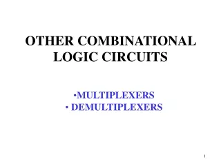
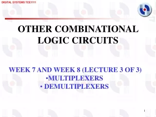
Combinational Logic Circuits. Binary Logic and Gates Logic Simulation Boolean Algebra Standard Forms Karnaugh Maps NAND/NOR and XOR gates. Read MK 29-80. Schematic for 4 Bit ALU. Invertor. AND Gate. EXOR Gate. OR Gate. 4. 2. 4. A. D. B. S. Simulation of 4 Bit ALU.

E N D
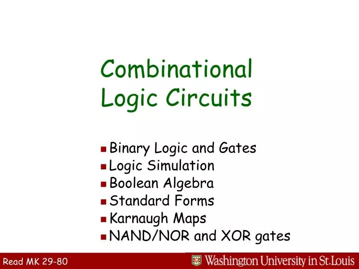
Combinational Logic Circuits • Binary Logic and Gates • Logic Simulation • Boolean Algebra • Standard Forms • Karnaugh Maps • NAND/NOR and XOR gates Read MK 29-80
Schematic for 4 Bit ALU Invertor ANDGate EXORGate ORGate
4 2 4 A D B S Simulation of 4 Bit ALU if S=0 then D=B-A if S=1 then D=A-B if S=2 then D=A+B if S=3 then D=-A
Elementary Binary Logic Functions • Digital circuits represent information using two voltage levels. • binary variables are used to denote these values • by convention, the values are called “1” and “0” and we often think of them as meaning “True” and “False” • Functions of binary variables are called logic functions. • AND(A,B) = 1 if A=1 and B=1, else it is zero. • AND is generally written in the shorthand A×B (or A&B or AÙB) • OR(A,B) = 1 if A=1 or B=1, else it is zero. • OR is generally written in the shorthand form A+B (or A|B or AÚB) • NOT(A) = 1 if A=0 else it is zero. • NOT is generally written in the shorthand form (or ØA or A) • AND, OR and NOT can be used to express all other logic functions.
EQUAL NAND NOR OR BÞA EXOR A ONE ZERO AND (BÞA) B A (AÞB) AÞB B A B 1111 0001 0000 1000 1100 0100 0010 0111 0101 1010 1110 1101 1011 0011 1001 0110 0011 0101 Two Variable Binary Logic Functions • Can make similar truth tables for 3 variable or 4 variable functions, but gets big (256 & 65,536 columns). • Representing functions in terms of AND, OR, NOT. • NAND(A,B) = (A×B) • EXOR(A,B) = (A×B) + (A×B)
Timing Diagram X X AND Gate X×Y Y Y X X×Y OR Gate X+Y Y X+Y Inverter X X’ X’ Basic Logic Gates • Logic gates “compute” elementary binary functions. • output of an AND gate is “1” when both of its inputs are “1”, otherwise the output is zero • similarly for OR gate and inverter • Timing diagram shows how output values change over time as input values change.
6 input OR Gate 3 input AND Gate A A A+B+C+D+E+F B B A×B×C C C D E F Multivariable Gates • AND function on n variables is “1” if and only if ALL its arguments are “1”. • n input AND gate output is “1” if all inputs are “1” • OR function on n variables is “1” if and only if at least one of its arguments is “1”. • n input OR gate output is “1” if any inputs are “1” • Can construct “large” gates from 2 input gates. • however, large gates can be less expensive than required number of 2 input gates
A B C B×C A+B×C 00001111 00110011 01010101 00100010 00101111 A B A+B×C C Elements of Boolean Algebra • Boolean algebra defines rules for manipulating symbolic binary logic expressions. • a symbolic binary logic expression consists of binary variables and the operators AND, OR and NOT (e.g. A+B×C) • The possible values for any Boolean expression can be tabulated in a truth table. • Can define circuit forexpression by combininggates.
Schematic Capture & Logic Simulation schematicentry tools schematic symbols wires gates signalwaveforms terminals signalnames
Installing CAD Tools xilinx.com/univ/ link to resource center
Accessing Installation Tutorial link to installation tutorial
Installation Tutorial Follow instructions carefully. It’s easy to do it right, but it’s even easier to do wrong! Go through tutorial and print each page before starting installation
Outline of Installation • Xilinx University page - http://xilinx.com/univ/index.htm • University resource center - http://xup.msu.edu/ • for installation tutorial - recommend you print this out first! • Problems/issues • disks may be mislabeled - tutorial says they are, mine weren’t • installation instructions included with disks may be wrong • modelsim is not included on the install disk, but is available on web site • Major steps – see tutorial for details • Find registration id on printed card with software • Install software and documentation • choose typical installation with all device types (default) • when MultiLinx driver dialog box comes up, just say no • Install the service pack from the Xilinx web site (use link on tutorial) • Install the IP update from the Xilinx web site (use link on tutorial) • Install ModelSim from the Xilinx web site (use link on tutorial) • select MXE Starter • license ModelSim
Starting New Project File New Project Specifyname and location • Start Project Navigatorby selecting • Start Programs Xilinx ISE 4 Project Navigator SpecifyVirtex 2 and XST VHDL
Starting New Project Project New Source Select Schematic enter name
Starting New Project zoom controls click here to create gate select and2
Starting New Project wiring tool IO pin tool add IO pins add wires
Starting New Project double-click for properties rename as desired
Simulating Circuit Project New Source select test bench waveform
Specifying Inputs to Circuit define input waveforms by clicking to create transitions note how all combinations of inputs are defined When saving enter 1. Comes up on startup - enter 10 in both and ns for Time Scale
Generating Expected Results double-click here to generate expected results expected results shown in HDL Bencher quit without saving finally, double-click here to do full simulation
Running Simulation restart and Run –all buttons zoom controls main ModelSim command window waveforms appear here
A A+B×C (B×(C)) Boolean Functions to Logic Circuits • Any Boolean expression can be converted to a logic circuit made up of AND, OR and NOT gates. step 1: add parentheses to expression to fully define order of operations - A+(B×(C)) step 2: create gate for “last” operation in expression gate’s output is value of expression gate’s inputs are expressions combined by operation step 3: repeat for sub-expressions and continue until done • Number of simple gates needed to implement expression equals number of operations in expression. • so, simpler equivalent expression yields less expensive circuit • Boolean algebra provides rules for simplifying expressions
Basic Identities of Boolean Algebra 2. X×1 =X 4. X×0 = 0 6. X×X=X 8. X×X’ = 0 11. X×Y=Y×X 13. X×(Y×Z) = (X×Y)×Z 15. X+(Y×Z) =(X+Y)×(X+Z) 17. (X×Y)’ = X+Y commutative associative distributive DeMorgan’s 1. X + 0 =X 3. X + 1 = 1 5. X + X=X 7. X + X’ = 1 9. (X’)’ =X 10. X + Y=Y + X 12. X+(Y+Z) = (X+Y)+Z 14. X(Y+Z) =X×Y + X×Z 16. (X+ Y)=X×Y • Identities define intrinsic properties of Boolean algebra. • Note: 15-17 have no counterpart in ordinary algebra. • Parallel columns illustrate duality principle. • Other handy identities. • A+AB=A (follows from 2, 14 and 3), A+A’B=A+B (15, 7 and 2)
X+(Y×Z) =(X+Y)×(X+Z) (X+ Y)=X×Y XYZ Y×Z X+(Y×Z) X+Y X+Z (X+Y)×(X+Z) XY (X+ Y) X×Y 00 1 1 000 0 0 0 0 0 0 01 0 0 1 0 0 0 001 0 10 0 0 0 010 0 1 0 0 11 0 1 011 1 1 1 1 1 1 1 100 0 1 1 101 0 1 1 1 0 110 1 1 1 1 1 111 1 1 1 1 Verifying Identities Using Truth Tables • Can verify any logical equation with small number of variables using truth tables. • Break large expressions into parts, as needed.
DeMorgan’s Laws for n Variables • We can extend DeMorgan’s laws to 3 variables by applying the laws for two variables. (X + Y + Z)=(X+ (Y + Z))- by associative law =X×(Y + Z)- by DeMorgan’s law =X×(Y×Z) - by DeMorgan’s law = X×Y×Z- by associative law (X×Y×Z)=(X×(Y×Z))- by associative law =X+ (Y×Z) - by DeMorgan’s law =X+ (Y+ Z)- by DeMorgan’s law = X+ Y+ Z- by associative law • Generalization to n variables. • (X1 + X2 + × × × + Xn)=X1×X2× × × Xn • (X1×X2× × × Xn)=X1 + X2 + × × × + Xn
X Y Z by identity 14 X Y F=XY(Z +Z)+XZ Z by identity 7 X F=XY×1+XZ =XY +XZ by identity 2 Y Z Simplification of Boolean Expressions F=XYZ+XYZ+XZ
The Duality Principle • The dual of a Boolean expression is obtained by interchanging all ANDs and ORs, and all 0s and 1s. • example: the dual of A+(B×C)+0 is A×(B+C)×1 • The duality principle states that if E1 and E2 are Boolean expressions then E1= E2 dual(E1)=dual(E2) where dual(E) is the dual of E. For example, A+(B×C)+0 = (B×C)+D A×(B+C)×1 = (B+C)×D • consequently, the pairs of identities (1,2), (3,4), (5,6), (7,8), (10,11), (12,13), (14,15) and (16,17) all follow from each other through the duality principle • also, A+AB=A A(A+B)=A & A+A’B=A+B A(A’+B)=AB
The Consensus Theorem Theorem. XY +YZ + XZ = XY + XZ Proof. XY +YZ + XZ = XY + (X + X)YZ + XZ2,7 = XY + XYZ + XYZ + XZ 14 = XY(1 + Z)+ XZ(Y +1) 2,11,14 = XY + XZ 3,2 Example. (A + B)(A+ C) = AA+ AC + AB + BC = AC + AB + BC = AC + AB Dual. (X + Y)(Y + Z)(X + Z) = (X + Y)(X + Z)
Taking the Complement of a Function Method 1. Apply DeMorgan’s Theorem repeatedly. (X(YZ+ YZ)) = X+ (YZ+ YZ) = X + (YZ)(YZ) = X+ (Y + Z)(Y+ Z) Method 2. Complement literals and take dual (X(YZ+ YZ))= dual(X(YZ + YZ)) = X+ (Y + Z)(Y+ Z)
Sum of Products Form • The sum of products is one of two standard forms for Boolean expressions. sum-of-products-expression = p-term+p-term ... +p-term p-term = literal×literal×××× ×literal • example. XYZ + XZ + XY + XYZ • A minterm is a term that contains every variable, in either complemented or uncomplemented form. • example. in expression above, XYZ is minterm, but XZ is not • A sum of minterms expression is a sum of products expression in which every term is a minterm. • example:XYZ + XYZ + XYZ + XYZ is sum of minterms expression that is equivalent to expression above. • shorthand: list minterms numerically, so XYZ + XYZ +XYZ + XYZ becomes 001+011+110+111 or Sm(1,3,6,7)
Simplifying Sum-of-Products Expressions • Sum of products forms yield 2 level AND-OR circuits. • Any expression can be put into sum of products form by applying distributive laws. • The simplest sum of products expression yields simplest 2 level AND-OR circuit. • Any Boolean expression can be viewed as a set of minterms. • An expression F covers another expression G, if the minterms in G are a subset of the minterms in F. • AC covers AB’C, since AC contains minterms 5 and 7 (from the set of 8 minterms on the variables A, B, and C) and AB’C contains only minterm 5.
General Simplification Procedure Given an expression F (e.g. ABD+AB+BCD+BCD+BCD). Step 1. Let M be the set of minterms covered by F. ABCD ABCD ABCD ABCD ABCD ABCD ABCD ABCD ABCD ABCD ABCD Step 2. For each minterm, m,find all maximal terms that cover m and also cover other minterms in M, but no minterms that are not in M. Let T be the resulting set of terms. (T={AB, BC, BD, CD, AC, BC}) Step 3. Select all terms in T that cover minterms covered by no other terms in T ({BC, BC}) Step 4. Select additional terms in T until selected terms cover all minterms. At each step, select a term that covers the largest possible number of new minterms. ({AB, CD})
CD 00 01 11 10 AB 0 0 1 1 00 1 1 1 1 01 1 1 1 0 11 0 0 1 1 10 CD CD CD 00 01 11 10 00 01 11 10 AB AB 00 01 11 10 AB 0 0 1 1 00 0 0 1 1 00 0 0 1 1 00 1 1 1 1 01 1 1 1 1 01 1 1 1 1 01 1 1 1 0 11 1 1 1 0 11 1 1 1 0 11 0 0 1 1 10 0 0 1 1 10 0 0 1 1 10 Simplification Using Karnaugh Maps Step 3. Select essential terms. Step 1. List all minterms covered by F. Step 2. Find maximal terms. Step 4. Cover remaining minterms.
CD 00 01 11 10 AB 0 0 0 1 00 1 1 0 1 01 1 1 1 1 11 1 0 1 1 10 CD BC 00 01 11 10 00 01 11 10 AB A 0 0 0 1 00 0 1 0 1 0 1 1 0 1 01 1 1 1 1 1 1 1 1 1 11 1 0 1 1 10 More Karnaugh Maps F=ABC+BC+ABC +BC F=A+BC+BC F=ABC+ACD+ABC+ABCD+ABC+ABC • Covering 0s gives complement of function. F=BC+CD+ AC+ AD F= ABC+BCD+ACD If we then take the complement of this expression, we get the product of sums form. F =(A+B +C)(B+C+D)(A+C+D)
Don’t Care Conditions • In some situations, we don’t care about the value of a function for certain combinations of the variables. • these combinations may be impossible in certain contexts • or the value of the function may not matter in when the combinations occur • In such situations we say the function is incompletely specified and there are multiple (completely specified) logic functions that can be used in the design. • so we can select a function that gives the simplest circuit • When constructing the terms of T in the simplification procedure, we can choose to either cover or not cover the don’t care conditions.
CD CD 00 00 01 01 11 11 10 10 AB AB 0 0 1 1 0 0 0 0 00 00 x x x x x x 1 1 01 01 1 1 1 1 1 1 x x 11 11 x x 0 0 1 1 1 1 10 10 Map Simplification with Don’t Cares F=ACD+B+AC • Alternative covering. F=ABCD+ABC+BC+AC
Product of Sums Form • The product of sums is the second standard form for Boolean expressions. product-of-sums-expression = s-term×s-term ... ×s-term s-term = literal+literal+××× +literal • example. (X+Y+Z )(X+Z)(X+Y)(X+Y+Z) • A maxterm is a sum term that contains every variable, in complemented or uncomplemented form. • example. in exp. above, X+Y+Z is a maxterm, but X+Z is not • A product of maxterms expression is a product of sums expression in which every term is a maxterm. • example.(X+Y+Z )(X+Y+Z)(X+Y+Z)(X+Y+Z)is product of maxterms expression that is equivalent to expression above. • shorthand: list maxterms numerically: so, (X+Y+Z )(X+Y+Z) (X+Y+Z)(X+Y+Z) becomes 110+100+001+000 or PM(6,4,1,0)
X X NAND Gate NOR Gate (X+Y) (X×Y) Y Y = = = = NAND and NOR Gates • In certain technologies (including CMOS), a NAND (NOR) gate is simpler & faster than an AND (OR) gate. • Consequently circuits are often constructed using NANDs and NORs directly, instead of ANDs and ORs. • Alternative gate representations makes this easier.
Pure NAND Implementation A EXOR gate A AB+AB B B Exclusive Or and Odd Function • The EXOR function is defined by AB = AB + AB. • The odd function on n variables is 1 when an odd number of its variables are 1. • odd(X,Y,Z) = XYZ+ XYZ + XYZ + XYZ = X Y Z • similarly for 4 or more variables • Parity checking circuits use the odd function to provide a simple integrity check to verify correctness of data. • any erroneous single bit change will alter value of odd function, allowing detection of the change
Integrated Circuits • Digital logic is implemented using transistors in integrated circuits containing many gates. • small-scale integrated circuits (SSI) contain 10 gates or less • medium-scale integrated circuits (MSI) contain 10-100 gates • large-scale integrated circuits (LSI) contain up to 104 gates • very large-scale integrated circuits (VLSI) contain >104 gates • Improvements in manufacturing lead to ever smaller transistors allowing more per chip. • >107 gates/chip now possible; doubles every 18-24 months • Variety of logic families. • TTL - transistor-transistor logic • CMOS - complementary metal-oxide semiconductor • ECL - emitter-coupled logic • GaAs - gallium arsenide
n-FET p-FET off n-FET on n-FET off p-FET on p-FET L L H H gate transmission gate NOR inverter NAND B (AB) A B (A+B) A TG CMOS Logic Gates • the gate (note different meaning) input controls whether current can flow between the other two terminals or not. • CMOS integrated circuits are built using two types of Field Effect Transistors (FET), n-type & p-type. • Logic gates are constructed by combining transistors in complementary arrangements.
X Y Z X Y Z Circuit Delays in CMOS Circuits • Electronic gates are physical devicesthat take time to operate. • Response to instantaneous change atX is gradual decrease in voltage atY and similar gradual increase at Z. • Voltage at Y must drop below logicthreshold level to be “seen” as a ‘0’. • This effect can be viewed as delay in propagation of logic values. • tPLH denotes low-to-high delay • tPHL denotes high-to-low delay • tpd= max{tPLH, tPHL} • relative values of tPLH and tPHL depend on relative “strength” of pull-up and pull-down transistors in inverters • values vary with operating temperature and manufacturing processes
equivalent circuitwhen X is low X Y Z Z Y X X Y Z equivalent circuitwhen X is high X Y Z Closer Look at CMOS Circuit Delays • When X goes high, pull-up of first inverter turns off and pull-down turns on. • Decrease of voltage at Y requires transfer of charge from capacitor to ground. • wires and transistor gates act like capacitors • time for transfer depends on size of capacitance and on resistance of pull-down transistor • pull-up & pull-down transistors can have different “on-state” resistance values • Use of two parallel inverters between X and Y can give faster logic transitions.
Negative Logic – What’s in a Name? • In positive logic systems, a high voltage is associated with a logic 1, and a low voltage with a logic 0. • positive logic is just one of two conventions that can be used to associate a logic value with a voltage • sometimes it is more convenient to use opposite convention • Circuits often have some signals that are “active low”. • a signal called “enable” may allow some operation to occur only when it is low • it’s good practice to label such signals explicitly to prevent confusion - e.g. enable.L • the name of a signal may determine if it’s viewed as active high or active low (for example enable.L=inhibit.H) • To avoid ambiguity, manufacturers generally specify components in terms of high and low voltage values.