Download
1 / 38
380 likes | 382 Vues
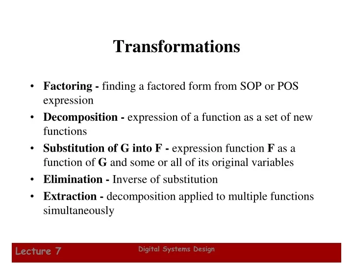
Transformations. Factoring - finding a factored form from SOP or POS expression Decomposition - expression of a function as a set of new functions Substitution of G into F - expression function F as a function of G and some or all of its original variables

E N D
Transformations • Factoring - finding a factored form from SOP or POS expression • Decomposition - expression of a function as a set of new functions • Substitution of G into F - expression function F as a function of G and some or all of its original variables • Elimination - Inverse of substitution • Extraction - decomposition applied to multiple functions simultaneously Digital Systems Design
Transformation Examples • Extraction • Beginning with two functions: E = A’B’D’+ A’BD H = B’CD’ + BCD G = 16 • Finding a common factor and defining it as a function: F = B’D’+ BD • We perform extraction by expressing E and H as the three functions: F = B’D’+ BD, E = A’F, H = CF G = 10 • The reduced cost G results from the sharing of logic between the two output functions Digital Systems Design
Example: • Multiple Output Minimization - Extraction: • F(A,B,C) = m(3,6,7) and G(A,B,C) = m(0,1,3) • Implement F and G using minimum number of gates. Digital Systems Design
Other Gate Types • Why? • Implementation feasibility and low cost • Power in implementing Boolean functions • Convenient conceptual representation • Gate classifications • Primitive gate - a gate that can be described using a single primitive operation type (AND or OR) plus an optional inversion(s). • Complex gate - a gate that requires more than one primitive operation type for its description Digital Systems Design
X F Buffer • A buffer is a gate with the function F = X: • In terms of Boolean function, a buffer is the same as a connection! • So why use it? • A buffer is an electronic amplifier used to improve circuit voltage levels and increase the speed of circuit operation. Digital Systems Design
X = × × F ( X , Y , Z ) X Y Z Y Z NAND Gate • The basic NAND gate has the following symbol, illustrated for three inputs: • AND-Invert (NAND) • NAND represents NOTAND, i. e., the AND function with a NOT applied. The symbol shown is an AND-Invert. The small circle (“bubble”) represents the invert function. Digital Systems Design
= + + F ( X , Y , Z ) X Y Z X Y Z NAND Gates (continued) • Applying DeMorgan's Law gives Invert-OR (NAND) • This NAND symbol is called Invert-OR, since inputs are inverted and then ORed together. • AND-Invert and Invert-OR both represent the NAND gate. Having both makes visualization of circuit function easier. • A NAND gate with one input degenerates to an inverter. Digital Systems Design
NAND Gates (continued) • The NAND gate is the natural implementation for the simplest and fastest electronic circuits • Universal gate - a gate type that can implement any Boolean function. • The NAND gate is a universal gate as shown in Figure 2-30 of the text. • NAND usually does not have a operation symbol defined since • the NAND operation is not associative, and • we have difficulty dealing with non-associative mathematics! Digital Systems Design
NAND Circuits • NAND is said to be universal gate Digital Systems Design
For easy conversion to NAND logic let’s define convenient representations: Digital Systems Design
Two-Level Implementation • If we have sum-of-products, it’s easy. • First level: AND gates • Second level: OR gates Digital Systems Design
F(X,Y,Z) = Digital Systems Design
X = + + F ( X , Y , Z ) X Y Z Y Z NOR Gate • The basic NOR gate has the following symbol, illustrated for three inputs: • OR-Invert (NOR) • NOR represents NOT - OR, i. e., the OR function with a NOT applied. The symbol shown is an OR-Invert. The small circle (“bubble”) represents the invert function. Digital Systems Design
X Y Z NOR Gate (continued) • Applying DeMorgan's Law gives Invert-AND (NOR) • This NOR symbol is called Invert-AND, since inputs are inverted and then ANDed together. • OR-Invert and Invert-AND both represent the NOR gate. Having both makes visualization of circuit function easier. • A NOR gate with one input degenerates to an inverter. Digital Systems Design
NOR Gate (continued) • The NOR gate is another natural implementation for the simplest and fastest electronic circuits • The NOR gate is a universal gate • NOR usually does not have a defined operation symbol since • the NOR operation is not associative, and • we have difficulty dealing with non-associative mathematics! Digital Systems Design
NOR Circuits • NOR : dual of NAND & also an universal gate Digital Systems Design
Exclusive OR/ Exclusive NOR • The eXclusive OR (XOR) function is an important Boolean function used extensively in logic circuits. • The XOR function may be; • implemented directly as an electronic circuit (truly a gate) or • implemented by interconnecting other gate types (used as a convenient representation) • The eXclusive NOR function is the complement of the XOR function • By our definition, XOR and XNOR gates are complex gates. Digital Systems Design
Å = + X Y X Y X Y Exclusive OR/ Exclusive NOR • Uses for the XOR and XNORs gate include: • Adders/subtractors/multipliers • Counters/incrementers/decrementers • Parity generators/checkers • Definitions • The XOR function is: • The eXclusive NOR (XNOR) function, otherwise known as equivalence is: • Strictly speaking, XOR and XNOR gates do no exist for more that two inputs. Instead, they are replaced by odd and even functions. Å = + X Y X Y X Y Digital Systems Design
Å Å X Y X Y X Y (X Y) º or X Y 0 0 0 0 0 1 0 1 1 0 1 0 1 0 1 1 0 0 1 1 0 1 1 1 Truth Tables for XOR/XNOR • Operator Rules: XOR XNOR • The XOR function means: X OR Y, but NOT BOTH • Why is the XNOR function also known as the equivalence function, denoted by the operator ? Digital Systems Design
XNOR: (X Y)’ = (X×Y’ + X’×Y)’ = (X’+Y) × (X+Y’) = X×Y + X’×Y’ • Consider three variable XOR gate: X Y Z = (X × Y’ + X’× Y) × Z’ + (X × Y + X’× Y’) × Z = X × Y’× Z’ + X’× Y × Z’ + X × Y × Z + X’× Y’× Z If only one of the variables is 1 or all are 1 then the output is 1. • Generalization: • For three or more variables XOR gate returns 1 if odd number of variables are 1. Digital Systems Design
X Y Z X Y Z X Y Z X Y Z X Y Z Å X 0 X X 1 X Å = = Å X X 0 X X 1 Å = X Y Y X Å Å ) = = Å Å Å Å Å Å ( X Y Z X ( Y Z ) X Y Z XOR/XNOR (Continued) • The XOR function can be extended to 3 or more variables. For more than 2 variables, it is called an odd function or modulo 2 sum (Mod 2 sum), not an XOR: • The complement of the odd function is the even function. • The XOR identities: Å Å = + + + = = Digital Systems Design
Symbols For XOR and XNOR • XOR symbol: • XNOR symbol: • Symbols exist only for two inputs Digital Systems Design
XOR and XNOR symbols Digital Systems Design
XOR Implementation • X Y = X × Y’ + X’× Y • XOR with NAND gates F = [((X × Y)’× X)’× ((X × Y)’× Y)’]’ = (X × Y)’× X + (X × Y)’× Y = (X’+Y’) × X + (X’+Y’) × Y = X × Y’ + X’× Y Digital Systems Design
Odd and Even Functions • The odd and even functions on a K-map form “checkerboard” patterns. • The 1s of an odd function correspond to minterms having an index with an odd number of 1s. • The 1s of an even function correspond to minterms having an index with an even number of 1s. • Implementation of odd and even functions for greater than 4 variables as a two-level circuit is difficult, so we use “trees” made up of : • 2-input XOR or XNORs • 3- or 4-input odd or even functions Digital Systems Design
X Y F Z + + + + Example: Odd Function Implementation • Design a 3-input odd function F =X Y Zwith 2-input XOR gates • Factoring, F = (X Y) Z • The circuit: Digital Systems Design
W X E = F’ Y Z + + + + + + Example: Even Function Implementation • Design a 4-input odd function F = W X Y Zwith 2-input XOR and XNOR gates • Factoring, F = (W X) (Y Z) • The circuit: Digital Systems Design
X Y P Z X Y E Z P Parity Generators and Checkers • Message : XYZ (3-bit) • Parity : (even parity) : P = X Y Z • Parity checker : E = X Y Z P Digital Systems Design
Multi-input XOR • Sum modulo 2 • Parity computation • Used to generate and check parity bits in computer systems. • Detects any single-bit error Digital Systems Design
Parity tree Digital Systems Design
Hi-Impedance Outputs • Logic gates introduced thus far • have 1 and 0 output values, • cannot have their outputs connected together, and • transmit signals on connections in only one direction. • Three-state logic adds a third logic value, • Hi-Impedance (Hi-Z), • giving three states: 0, 1, and Hi-Z on the outputs. • The presence of a Hi-Z state makes a gate output as described above behave quite differently: • “1 and 0” become “1, 0, and Hi-Z” • “cannot” becomes “can,” and • “only one” becomes “two” Digital Systems Design
Hi-Impedance Outputs (continued) • What is a Hi-Z value? • The Hi-Z value behaves as an open circuit • This means that, looking back into the circuit, the output appears to be disconnected. • It is as if a switch between the internal circuitry and the output has been opened. • Hi-Z may appear on the output of any gate, but we restrict gates to: • a 3-state buffer, or • a transmission gate, each of which has one data input and one control input. Digital Systems Design
IN OUT EN EN IN OUT 0 X Hi-Z 1 0 0 1 1 1 The 3-State Buffer Symbol • For the symbol and truth table, IN is the data input, and EN, the control input. • For EN = 0, regardless of the value on IN (denoted by X), the output value is Hi-Z. • For EN = 1, the output value follows the input value. • Variations: • Data input, IN, can be inverted • Control input, EN, can be inverted by addition of “bubbles” to signals. Truth Table Digital Systems Design
Resolving 3-State Values on a Connection • Connection of two 3-state buffer outputs, B1 and B0, to a wire, OUT • Assumption: Buffer data inputs can take on any combination of values 0 and 1 • Resulting Rule: At least one buffer output value must be Hi-Z. Why? • How many valid buffer output combinations exist? • What is the rule for n 3-state buffers connected to wire, OUT? • How many valid buffer output combinations exist? Digital Systems Design
3-State Logic Circuit • Data Selection Function: If s = 0, OL = IN0, else OL = IN1 • Performing data selection with 3-state buffers: • Since EN0 = S and EN1 = S, one of the two buffer outputs is always Hi-Z plus the last row of the table never occurs. IN0 OL EN0 S IN1 EN1 Digital Systems Design
X Y C C 1 and C 0 = = (b) X TG Y Y X TG X Y C 0 and C 1 = = C (c) (a) C (d) Transmission Gates • The transmission gate is one of the designs for an electronic switch for connecting and disconnecting two points in a circuit: Digital Systems Design
Transmission Gates (continued) • In many cases, X can be regarded as a data input and Y as an output. C and C, with complementary values applied, is a control input. • With these definitions, the transmission gate, provides a 3-state output: • C = 1, Y = X (X = 0 or 1) • C = 0, Y = Hi-Z • Care must be taken when using the TG in design, however, since X and Y as input and output are interchangeable, and signals can pass in both directions. Digital Systems Design
+ Circuit Example Using TG • Exclusive OR F = A C • The basis for the function implementation is TG-controlled paths to the output Digital Systems Design