Download
1 / 10
100 likes | 180 Vues
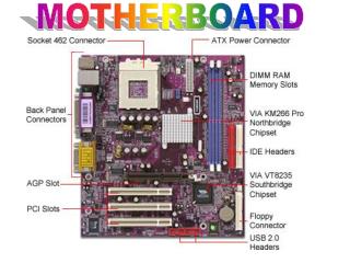
HPS Motherboard Electronic Design. 4 PCB: LEFT TOP 115 channels, LEFT BOTTOM (115), RIGHT TOP (106), RIGHT BOTTOM (106). For LEFT TOP board 115 channels we have:

E N D
HPS Motherboard Electronic Design • 4 PCB: LEFT TOP 115 channels, LEFT BOTTOM (115), RIGHT TOP (106), RIGHT BOTTOM (106). • For LEFT TOP board 115 channels we have: • 115 smd connectors (AMP 10 pin)for preamp very similar to previous version (pin slightly smaller). It is the same of FT-Cal motherboard. • 15 TE signal connectors from 16 pin each, equal to previous version. • 2 HV connectors (15 pin) DSUB 750V, 5A, trough hole different to previous for a easier routing. • 1 LV connectors (6 pin). • We can use a very similar HV grouping. • We can use the same cable as discussed with Stepan Stepanyan.
HPS Motherboard Layout Design • 4 PCB: LEFT TOP 115 channels, LEFT BOTTOM (115), RIGHT TOP (106), RIGHT BOTTOM (106). • Board Dimension is 400x240 mm and 143 component each. • Board Thickness = 2.5 mm. • Layout specifications: • 10 Layers (3 signals + 1 for High Voltage + 1 fan-out + 5 GND). • 115 signal traces with 50 Ohms impedance. • Signal: 0.2 mm line width and 0.2 mm min. spacing. • HV: 0.5 mm line width and 0.8 mm min. spacing. • Ground ring between two signals.
HPS Motherboard Next Steps • Mechanical Specifications with Orsay. Done! • Design of LEFT TOP and LEFT BOTTOM boards. Done! • Layout routing of LEFT TOP and LEFT BOTTOM boards. NOW • Design of RIGHT TOP and RIGHT BOTTOM boards with the correct HV grouping. November. • Layout routing of RIGHT TOP and RIGHT BOTTOM boards. • End of year. • Board Productions and Assembly (with the same company used for the FT-Cal). rough estimate 5Keuro. January 2014. • Test on Electrical connections and Full crosstalk test with FT-Cal crystals. February 2014.