Download
1 / 9
90 likes | 206 Vues
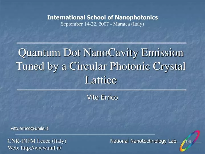
Quantum Dot NanoCavity Emission Tuned by a Circular Photonic Crystal Lattice. International School of Nanophotonics September 14-22, 2007 - Maratea (Italy). Vito Errico. vito.errico@unile.it. CNR-INFM Lecce (Italy) National Nanotechnology Lab Web: http://www.nnl.it/ . Outline.

E N D
Quantum Dot NanoCavity Emission Tuned by a Circular Photonic Crystal Lattice International School of Nanophotonics September 14-22, 2007 - Maratea (Italy) Vito Errico vito.errico@unile.it CNR-INFM Lecce (Italy) National Nanotechnology Lab Web: http://www.nnl.it/
Outline • State of the art on nanocavities and whispering gallery devices • Standard photonic crystals vs Circular photonic crystals (CPC) • Simulations of 2D CPC cavity • Fabrication of membrane QD cavity • Optical characterization of 2D-CPC Nano-Resonator
Experimental QDs epitaxially growth by molecular beam epitaxy (MBE) Ground state QD emission around 1288nm Dot density: 3.2·1010 cm-2
Experimental Electronic exposure and resist development • Acceleration voltage: 20 keV • Aperture size: 7.5 • Dose: 38 mC/cm2 • Circular mode and Proximity Error Correction (PEC) were used Dry-etching by ICP plasma etching • Gas involved: SiCl4/He (16sccm/4sccm) • Platen power: 60W • Pressure: 2mtorr Sacrificial layer removal by wet-etching • HF:H2O (1:10) at room temperature
Fabrication Results SEM image of the nano-cavity after processing procedure Brighter area corresponds to Al0.7Ga0.3As removal The four rectangles on each side of the nano-cavity structure assist wet-etching process [1] V. Errico et al. / Microelectronic Engineering 84 (2007) 1570–1573
Fabrication Results SEM image of totally suspended nano-cavity after processing procedure
Optical Characterization Results Cavity parameter: a:350nm ri/a = 0.47 ro/a = 0.67 Peak: Center: 1282nm FWHM: 0.62nm Quality factor: Q≈2000 [2] V. Errico, et al., High-Q factor single mode circular photonic crystal nano-resonator, Superlattices and Microstructures (2007), doi:10.1016/j.spmi.2007.06.013
Conclusion • Circular nano-cavities behaviour has been simulated to match cavity resonance and QDs emission. • CPC device based on air/GaAs/air membrane has been realized. • QDs Nano-Cavity emission has been tuned by a circular photonic crystal lattice This technology is being applied to: • Whispering gallery modes device CPC technology based • Electrical injected CPC laser