Download
1 / 1
10 likes | 133 Vues
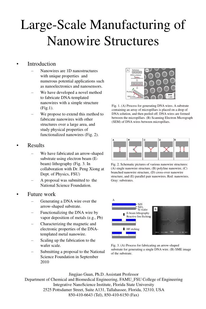
A. Substrate. B. DNA solution. Peeling. DNA wire. 1 u m. Large-Scale Manufacturing of Nanowire Structures. Introduction Nanowires are 1D nanostructures with unique properties and numerous potential applications such as nanoelectronics and nanosensors.

E N D
A Substrate B DNA solution Peeling DNA wire 1 um Large-Scale Manufacturing of Nanowire Structures • Introduction • Nanowires are 1D nanostructures with unique properties and numerous potential applications such as nanoelectronics and nanosensors. • We have developed a novel method to fabricate DNA-templated nanowires with a simple structure (Fig.1). • We propose to extend this method to fabricate nanowires with other structures over a large area, and study physical properties of functionalized nanowires (Fig. 2). • Results • We have fabricated an arrow-shaped substrate using electron beam (E-beam) lithography (Fig. 3. In collaboration with Dr. Peng Xiong at Dept. of Physics, FSU) • A proposal was submitted to the National Science Foundation. • Future work • Generating a DNA wire over the arrow-shaped substrate. • Functionalizing the DNA wire by vapor deposition of metals (e.g., Pb) • Characterizing the magnetic and electronic properties of the DNA-templated metal nanowire. • Scaling up the fabrication to the wafer scale. • Submitting a proposal to the National Science Foundation in September 2010 Fig. 1. (A) Process for generating DNA wires. A substrate containing an array of micropillars is placed on a drop of DNA solution, and then peeled off. DNA wires are formed between the micropillars. (B) Scanning Electron Micrograph (SEM) of DNA wires between micropillars. Fig. 2. Schematic pictures of various nanowire structures: (A) single nanowire structure, (B) polyline nanowire, (C) branched nanowire structure, (D) cross-over nanowire structure, and (E) parallel pair nanowires. Red: nanowires. Gray: substrates. A SiN SiO2 B Si wafer E-beam lithography Reactive Ion Etching HF etching Fig. 3. (A) Process for fabricating an arrow-shaped substrate for generating a single DNA wire. (B) SME image of the substrate. Jingjiao Guan, Ph.D. Assistant Professor Department of Chemical and Biomedical Engineering, FAMU_FSU College of Engineering Integrative NanoScience Institute, Florida State University 2525 Pottsdamer Street, Suite A131, Tallahassee, Florida, 32310, USA 850-410-6643 (Tel), 850-410-6150 (Fax)