Download
1 / 24
240 likes | 419 Vues
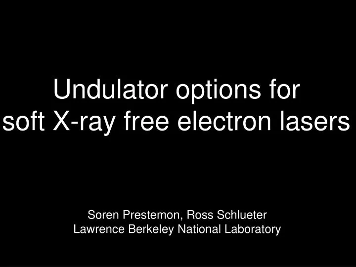
Undulator options for soft X-ray free electron lasers. Soren Prestemon, Ross Schlueter Lawrence Berkeley National Laboratory. Outline . Introduction Undulator technologies Permanent magnet & Superconducting Planar, helical, and variable polarization

E N D
Undulator options for soft X-ray free electron lasers • Soren Prestemon, Ross Schlueter • Lawrence Berkeley National Laboratory
Outline • Introduction • Undulator technologies • Permanent magnet & Superconducting • Planar, helical, and variable polarization • from “robust”, to “near-term development”, to “futuristic” • Performance comparison • Impact on overall facility design • Technical issues to be addressed
Introduction • Strong interest in a soft X-ray FEL facility • High (~MHz) pulse repetition rate (see F. Sannibale) • CW SCRF linac • Multiple (~10) FEL lines feeding independent experiments “R&D for a Soft X-Ray Free Electron Laser Facility” Joint LBNL / SLAC Whitepaper, June 2009
Cryogenics+linacand Undulator lines are dominant cost drivers Importance of undulator technology • Undulator characteristics and beam energy yield photon wavelength • Coupled problem: • Always want tunability • Sometimes want polarization control • Different FEL lines will focus on different spectral ranges, with different timing, synchronization etc. needs
Overview: Technologies ALS EPU50 (1998) Pure permanent magnet technology, Elliptically polarizing capability ALS U50 (1993) Hybrid permanent magnet technology ALS SCU (20??) Nb3Sn superconducting undulator Spring8 IVUN (2000) Small gap In-vacuum device
Overview: Comparison of technologies SRC electromagnet undulator LCLS PM undulator Accel SC undulator
Undulator applications: storage ring vs. FEL • Storage ring: • gap>5mm (sometimes smaller...) • depends on β-function • introduce superimposed matching fodo lattice - very narrow gap? • Requires “large-midplane” • large horizontal dynamic aperture - effectively eliminates bifilar-helical devices • “Transparency” issues: • should be steering and displacement-free • must avoid coupling: skew terms an issue • dynamic multipoles must be compensated • FEL’s: • gap>4mm ->2mm? • limited by wakefields, vacuum, fabrication? • More restrictive trajectory requirements • fewer “knobs” to compensate for tuning/polarization-induced trajectory variations • Multipole fields - needs analysis
Overview: Ongoing developments(undulators only; misc. applications) Schlueter, in “Synch. Rad. Sources”, Ed. H. Winick, 1994 • Diverse spectral properties • quasi-periodicity, variable polarization: EM, PM; SC • In-vacuum permanent magnets • allows reduced gap => higher field • cryogenic PM => leverage increase in Br, enhanced coercivity • Superconducting • short-period helical, for ILC (~12-14mm period) • Daresbury: NbTi • APS: NbTi, considering Nb3Sn • short-period planar (typically ~15mm period) • LBNL: Nb3Sn • APS: NbTi, Nb3Sn • BNL: APS NbTi • ANKA: • NbTi; first device installed in ring, worked with Accel • Now investigating Nb3Sn with CERN • others...
Focus on superconducting devices - Push for highest performance - Leverage material developments Novel concepts: Issues for soft X-ray FEL’s • Approaches: • Focus on “solid-state” technologies • Leverage fabrication techniques: • minimize manual involvement • design for best tolerances • Build-in correction capability • Investigate in-situ tuning • Issues to be addressed: • Performance: • higher field and/or shorter periods • enhanced spectral range • variable polarization • Ease / reliability of manufacturing • quality control: tolerances, reproducibility • measurements, trajectory correction • Integration of electron-bunch controls • focussing magnets, collimation, diagnostics • Minimize overall system cost
D. Arbelaez, S. Caspi S. Caspi, PAC 1995 Performance: short-period concepts • Bifilar helical approaches yield excellent performance: • applicable for “short” periods, λ>~10 (7?) mm, gap>~3-5mm • wire dimensions, bend radii, and insulation issues • well-known technology (e.g. Stanford FEL Group, 1970’s), but not “mature” • most effective modulator for FEL • need to consider seed-laser polarization • currently being investigated for positron source production • NbTi (Europe), Nb3Sn (Argonne)
PM Hybrid SCU helical Vacuum aperture ~4mm Performance characteristics
λ1=1nm gap=4-5mm Impact on beam energy selection
A. Madur, F. Trillaud: see SRI 2009, Sydney, Australia B Switch 1 Switch 2 I A C Iload Switch 3 Switch 4 D R&D results for planar SCU’s at LBNL (mainly LBNL LDRD funds) Supported by APS WFO contract • Demonstrated performance • supports predictions of B(gap,period) • Demonstrated shim field • sufficient amplitude based in anticipated tolerances • Demonstrated “switch network” • reliably switch currents +, -, or off for each shim • allows fast commissioning of SCU • relevant for period-doubling schemes
Question: can a new approach simultaneously address: - performance issues - tolerance issues - cost issues Pushing performance limits • Technologies missing to reach ~5-8mm regime (or shorter!) • gap/period dictates performance • wire-based technologies reach limit due to: • finite wire size - winding becomes impractical • insulation does not scale • effective current density decreases • Need a new approach: • leverage microfabrication techniques • leverage strengths of new materials
Other superconducting materials Plot from Peter Lee, ASC-NHMFL
Consider stacked YBCO tapes • use micro-machining or lithography to produce current path • highly reproducible periodicity • low labor cost • stacked tapes operate in series • joints at ends • 20-30 tapes sufficient • large tolerance to stack errors • Current at edges largely cancels layer-to-layer; result is “clean” transverse current flow Consider new materials • Material (YBCO) is in the form of a “tape” • ~1 micron YBCO layer carries the current • does not scale: benefit drops with increased thickness • Critical temperature ~100K • 12mm wide tape carries ~300A at 77K • factor 5-10 higher at 4.5K, depending on applied field
Performance curves (calculated) • The HTS short period technology compared to PM and hybrid devices: • Scaling shows regions of strength of different technologies • Assumed Br=1.35 for PM and hybrid devices • Data shown for HTS assumes J=2x10⁵A/mm2, independent of field • For B>~1.5T, scaling needs to be modified to include J(B) relation • Issues considered: • Width of current path - assumed ~1mm laser cuts separating “turns” • Finite-length of straight sections – 83% retained for g=2mm, 12mm wide tape • Gap-period region of strength – most promising in g<3mm, l<10mm regime • Peak field on conductor & orientation - <~2.5T HTS: 2-2.2mm gap Helical: 3-3.2mm gap, 2kA/mm2 IVID PM: 2-2.2mm gap HTS low Cu HTS baseline Hybrid PM Pure PM Helical
Implications for FEL design A. Zholents K=1.4 K=1.2 K=1.0 K=0.8 • High fields at small periods allows access to 1nm with ~1.3GeV beam • Multiple routes for technology enhancements: • reduce tape thickness - work with vendor • increase YBCO layer thickness - collaborate with LANL / vendor
Aside: Micro-undulator concept • Push stacked-tape concept to a new level: • Concept: • Layered YBCO using micro-fabrication • Layers separated by ~5-10 microns • Series connection (i.e. joints) integrated in process • Eliminate almost all manual assembly • Period ~0.5-2mm • Gap ~200 microns Trial mask/deposition underway, in collaboration with LANL groupMPA-STC
A/mm2 Theoretical performance of YBCO micro-undulator • Assumptions: • 25 layers • gap=200 μm • 10 μm layer separation • no Jc(B) dependence included
Challenges of the HTS concepts • Shielding device from synchrotron radiation • Image current impact due to narrow gap • Beam dynamics / image current interaction with superconductor • Field errors are key challenge for all technologies: • Pros for HTS concept: • Possibly reduced longitudinal “assembly” tolerances • Laser/lithography cuts define periodicity • Layer-to-layer longitudinal placement not critical • No difficulty with longer lengths • Basic assembly very simple • Error calculations analytic • Cons for HTS concept: • Small gap requirement calls for integrated vac. Chamber • Vertical placement of layers must be consistent • Magnetization effects may cause unwanted field kicks • homogeneity of YBCO layer dictates reproducibility of current path • needs to be measured, controlled
Summary (1) “Tabletop” FEL’s tape micro-undulator HTS tape undulator SCU: Planar, helical ??? Cryogenic in-vac. hybrid Hybrid SC-EPU PM EPU
Lei Zang, Cockcroft Institute presentation Advanced undulators could address two dominant cost drivers of an FEL: the linac and the undulators Summary II: Critical research needs • SCU - planar and bifilar helical: • demonstrate reliable winding, reaction, and potting process for Nb3Sn • develop trajectory correction method • magnetic measurements • Stacked HTS undulator: • demonstrate effective J (i.e. B) • evaluate image-current issues • determine field quality / trajectory drivers • current path accuracy, J(x,y) distribution • accuracy of stacking • develop field correction methods • consider outer layer devoted to field correction (e.g. ANKA passive shim) • Stacked HTS Micro-undulator: • demonstrate ability to fabricate layers • demonstrate effective J (i.e. B) • evaluate image-current issues • SC-EPU • develop integrated switch network • Demonstrate performance
Field strength of planar devices: Nb3Sn~40% higher than NbTi NbTi~best theoretical CIVID (assume same vacuum aperture) Technology comparison: Planar devices Calculations for 15mm-period devices