Download
1 / 1
10 likes | 117 Vues
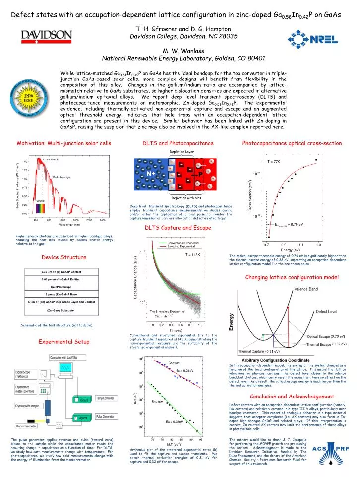
0.05 m m n+ (S) GaAsP Contact. 0.01 m m n+ (S) GaInP Emitter. GaInP Interrupt. 2 m m p (Zn) GaInP Base. -. -. -. -. -. -. -. -. -. -. -. -. -. -. -. -. -. -. -. -. -. -. -. -. +. -. -. -. -. -. -. -. +. +. +. +.

E N D
0.05 mm n+ (S) GaAsP Contact 0.01 mm n+ (S) GaInP Emitter GaInP Interrupt 2 mm p (Zn) GaInP Base - - - - - - - - - - - - - - - - - - - - - - - - + - - - - - - - + + + + 5 mm p+ (Zn) GaAsP Step Grade Layer and Contact + + + + + + (0.70 eV) (Zn) GaAs Substrate (0.32 eV) (0.21 eV) Depletion Layer N+ P Depletion with bias Defect states with an occupation-dependent lattice configuration in zinc-doped Ga0.58In0.42P on GaAs T. H. Gfroerer and D. G. Hampton Davidson College, Davidson, NC 28035 M. W. Wanlass National Renewable Energy Laboratory, Golden, CO 80401 While lattice-matched Ga0.51In0.49P on GaAs has the ideal bandgap for the top converter in triple-junction GaAs-based solar cells, more complex designs will benefit from flexibility in the composition of this alloy. Changes in the gallium/indium ratio are accompanied by lattice-mismatch relative to GaAs substrates, so higher dislocation densities are expected in alternative gallium/indium epitaxial alloys. We report deep level transient spectroscopy (DLTS) and photocapacitance measurements on metamorphic, Zn-doped Ga0.58In0.42P. The experimental evidence, including thermally-activated non-exponential capture and escape and an augmented optical threshold energy, indicates that hole traps with an occupation-dependent lattice configuration are present in this device. Similar behavior has been linked with Zn-doping in GaAsP, raising the suspicion that zinc may also be involved in the AX-like complex reported here. Motivation: Multi-junction solar cells DLTS and Photocapacitance Photocapacitance optical cross-section Deep level transient spectroscopy (DLTS) and photocapacitance employ transient capacitance measurements on diodes during and/or after the application of a bias pulse to monitor the capture/emission of carriers into/out of defect-related traps. DLTS Capture and Escape Higher energy photons are absorbed in higher bandgap alloys, reducing the heat loss caused by excess photon energy relative to the gap. Device Structure The optical escape threshold energy of 0.70 eV is significantly higher than the thermal escape energy of 0.32 eV, supporting an occupation-dependent lattice configuration model like the one shown below. Changing lattice configuration model The Stretched Exponential: Schematic of the test structure (not to scale). Conventional and stretched exponential fits to the capture transient measured at 143 K, demonstrating the non-exponential response and the suitability of the stretched exponential analysis. Experimental Setup In the occupation-dependent model, the energy of the system changes as a function of the local configuration of the lattice. This means that lattice vibrations, or phonons, can push the defect level closer to the valence band, but photons, which carry very little momentum, have no effect on the defect level. As a result, the optical escape energy is much larger than the thermal activation energies. Conclusion and Acknowledgement Defect centers with an occupation-dependent lattice configuration (namely, DX centers) are relatively common in n-type III-V alloys, particularly near bandgap crossover. This report of analogous behavior in p-type material suggests that acceptor complexes (i.e. AX centers) may also form in Zn-doped high-bandgap GaInP and related alloys. If this interpretation is correct, Zn-related AX centers may limit the performance of these alloys in photovoltaic cells. The pulse generator applies reverse and pulse (toward zero) biases to the sample while the capacitance meter reads the resulting change in capacitance as a function of time. For DLTS, we study how dark measurements change with temperature. For photocapacitance, we study how cold measurements change with the energy of illumination from the monochromator. The authors would like to thank J. J. Carapella for performing the MOVPE growth and processing the devices. Acknowledgment is made to the Davidson Research Initiative, funded by The Duke Endowment, and the donors of the American Chemical Society – Petroleum Research Fund for support of this research. Arrhenius plot of the stretched exponential rates (k) used to fit the capture and escape transients. We obtain thermal activation energies of 0.21 eV for capture and 0.32 eV for escape.