Download
1 / 11
110 likes | 112 Vues
PCB Designing is the most important activity in the process of designing and producing electronic products. In this infographic we have summarized the most important phases of PCB design, for all types of printed circuit boards and for all types of products

E N D
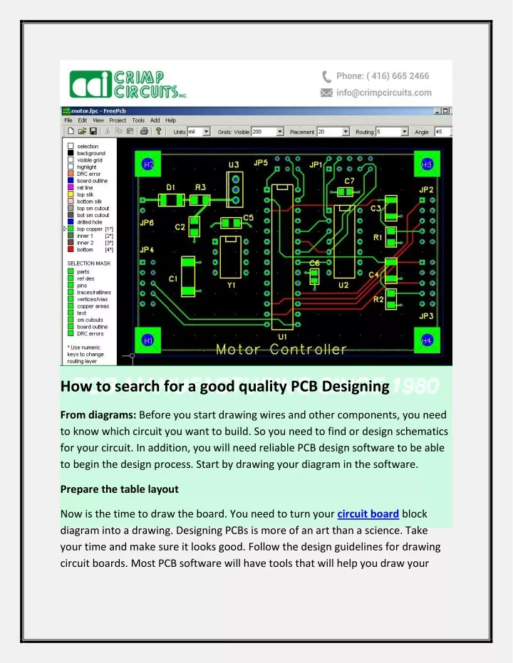
How to search for a good quality PCB Designing From diagrams: Before you start drawing wires and other components, you need to know which circuit you want to build. So you need to find or design schematics for your circuit. In addition, you will need reliable PCB design software to be able to begin the design process. Start by drawing your diagram in the software. Prepare the table layout Now is the time to draw the board. You need to turn your circuit board block diagram into a drawing. Designing PCBs is more of an art than a science. Take your time and make sure it looks good. Follow the design guidelines for drawing circuit boards. Most PCB software will have tools that will help you draw your
board from the schematic. We can't cover them all, but with further research we will find it is quite easy. Things to consider An important thing to consider is whether you are going to place the circuit board in a box? Remember that large components must be laid flat to accommodate. With a drawing of your components placed on your board, print it out on a sheet of paper. Use this paper version of your card to check if it fits in the box or if your connectors do. Have your PCB manufactured When you are done drawing your board, it's time to prepare your PCB for fabrication. This means you need to check your card for errors and convert your presentation to Gerber files. Then choose an affordable PCB maker and get your board ready. Detailed instructions This is just an introduction to PCB design. Learning the basics first will help you work on larger projects as you go along. Soon you will be able to work on advanced technologies like quad copters, LCD screens, and other awesome gadgets. Design Rule Checking Design Rule Checking (DRC) is the process aimed at verifying that the design rules have not been violated in an electronic project. These rules are the geometric constraints imposed on designers of printed circuit boards, semiconductor devices and integrated circuits (ICs), to ensure that their designs work correctly, as well as reliably, and can be produced with acceptable yield. The DRC is an important step in the context of the signoff that is the set of checks on the physical aspects of a project, which also includes LVS checks (layout versus schematic), XOR checks, ERC (check of the electrical rules) and controls of the 'antenna.
To simplify as much as possible, the following diagram shows what are the typical basic checks that must be made on the PCB layout: check that the width of the track is sufficient, that it is the spacing between adjacent tracks and that the copper perimeter of a pitch both regular and of sufficient thickness. 10 BEST PCB DESIGNING 1. KiCAD: KiCAD is open software that has a lot of features for its users such as output for Gerber Files, layout design of PCB, and schematic design and other good quality stuff. About the software tool is more powerful than the normal software and it has been designed in a way to achieve multitasking which is needed by an engineer for automation of design. This PCB design tool is supported by iOS X, Linux, and Windows.
2. DesignSpark PCB: The DesignSpark is known for its easy task for learning. It has features such as layout and schematic design of printed circuit boards. This software is used by a broad spectrum of users starting from beginners, students, and professionals. This software is free and it has 3D utility. 3. Express SCH and ExpressPCB Plus: Such a popular PCB design tool which is very easy to install. The process of its learning is very easy and it is also very easy to use. This software is capable of handling PCBs up to 4 layers. Good quality and rapid action.
4. Osmond PCB: About Osmond PCB is a dedicated OSX software tool and can run on Mac computers only. This tool has a great spatial resolution of about 10 nanometers.
5. Zenit PCB: Also this software is easy to use. It’s design is really creative in a quick fashion through it. This kind of software can be used by students with an easy efficiency. This software doesn’t have an auto-router which makes it tough to convert schematics in to layout, it can be used for Windows machines.
6. FreePCB: This software doesn’t have an auto-tracer or auto-router, but it can make use of an extension if downloaded known as “FreeRoute” which is an auto-router based on web. This software tool was released by famous GNU general public license. The software can be used by windows accounts. 7. Fritzing: This is a unique software tool which is supported by a web-based community and is mostly used for teaching electronics circuitry. This aim of this software tool is to create a very creative platform for users where they can learn electronics and
make layouts of printed circuit boards. This tool is very useful for beginners and students. User can use this software through many operating systems such as OSC, windows, and Linux. 8. TinyCAD: Basic software tools for making electronic schematics and its PCB layouts. This tool is an extended version of libraries for facilitating its users for PCB layout creations. One of the best features of this software is that it can be used front end to various other PCB layout software. There is an option for checking flaws in the PCB layout, only used by Windows accounts.
9. gEDA: About this software is a complete Electronic Design Automation software which is running on Linux operating systems only. This is entirely free and has capability of performing schematics, BOM list creation, attribute management, digital and analog simulation along with PCB layout creation.
10. BSch3V: This software tool is designed only for windows environment only. The BSch in its name stands for basic schematics. It’s the 3rd generation of the Suigyodo’s schematics software. But it has a limitation; there is not enough space to stock things.
Read more: https://www.crimpcircuits.com/blog/how-to- search-for-a-good-quality-pcb-designing/