Download
1 / 41
430 likes | 554 Vues
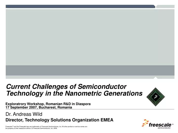
Current Challenges of Semiconductor Technology in the Nanometric Generations. Exploratrory Workshop, Romanian R&D in Diaspora 17 September 2007, Bucharest, Romania. Dr. Andreas Wild Director, Technology Solutions Organization EMEA. Content. Scaling More Moore Lithography

E N D
Current Challenges of Semiconductor Technology in the Nanometric Generations Exploratrory Workshop, Romanian R&D in Diaspora 17 September 2007, Bucharest, Romania • Dr. Andreas Wild • Director, Technology Solutions Organization EMEA
Content • Scaling • More Moore • Lithography • Transistor scaling • Interconnect • Power • More than Moore • Manufacturing • Conclusions
? ? Scaling : Moore’s Law Scaling: smaller features + larger wafers = diminishing cost Feature Size (nm) Wafer Size (mm) Average Transistor Cost • ITRS 2007 Edition: Affordable Cost per Function in 10 years • Packaged, ½ pitch 16nm • Transistor in MPU : $19n • DRAM bit : $1n
Scaling Improves Transistors, Enables Better Products Product Functionality Battery Life Power Consumption • Functionality to the Consumer means… • Longer battery life • Streaming video • Better phone graphics • Longer Phone Ranges • More memory for your digital camera • Faster, smaller portable computers • Laptops which won’t burn your lap • … Anything you can imagine… Portable, Longer Lasting Electronics Which Do More Things! =
Lithography • - 193nm still used • Immersion • Double exposure • Model-based OPC • Insolation • - EUV and eBeam still suffering of known problems
MOS Transistor Scaling Challenges • On chip in 10 years: • 275Gbit, 6BTransistors • - Lateral scaling • * Lithography • - Vertical scaling • * Leakage : high-k dielectric • * Gate material • - Performance enhancement • - Reliability • - Yield
NiSiGe SiGe Transport : SiGe, Parasitics : “Suitable Metal” NiSi Contacts on SiGe TEM SiGe 90% Si ref. 67% 20% Improvement 50% Cumulative Percentage 33% 10% 10 12 14 16 18 M1-P+ Resistance (Ohm/via)
Speed 40nm-thick Strained-Si Buried Insulator 30% higher performance 40% improved power Substrate Gate Parasitics S-SOI Reduced extrinsic resistance (ErSi, PtSi) Low K spacers msec anneals Strained Si Leakage Reliability, Yield Transistor and Process Challenges
Gate Leakage Control Thicker gate oxide with a higher dielectric constant will reduce leakage while keeping the electrostatic properties : Cox = keoA/dox
NMOS PMOS Gate Materials CV characteristics of ALD HfO2 and SiO2 core devices Changing polysilicon doping from n+ to p+ shifts its Fermi level from the conduction band edge to the valence band edge : - SiO2 CV curves shift by about 1V - HfO2 curves show little shift (0.13V, respectively 0.24V) → Fermi level pinning
Materials to Study for Gate Dielectric Shown in RED Good mid-gap metals, good N-channel metals, is P-channel still a problem ? Materials to Study for Gate Electrode shown in RED
Int. #2 Si ref. 380 A NiSiGe +20% NiSiGe SiGe SiGe SiGe Si BOX 400 500 600 700 800 Id,sat (A/m) Speed : Strain
Gate Last = no thermal budget issues Dual Gate Integration FSL, IEDM 2002
Fin Profile MG Metal Gate Multi Fin SRAM The Promise of the FinFET Architecture • FinFET integration showing : • Single Gate • Multi Gates • Independent Gates • Midgap Metal Gate and undoped channel (FD) Devices • Calibrated circuit simulation show 34% Fmax increase at 1.1v • Enable new circuits and application beyond the planar devices
Impact of Random Fluctuation on SRAM functionality(MASTAR Simulation) Lower doping => less fluctuations
Interconnect MOS Transistor Scaling: Transistors and Interconnections
Interconnect Scaling Challenges • On chip in 10 years: • > 35km interconnect • > 20 billion vias • Challenges • - Performance (switching delay ~RC) • * Resistance : • Material : aluminium – copper – • nanotubes ? • Cross section : deposition • * Parasitic capacity : low-k • dielectrics • - Reliability • * cleaning • * enhancement – barrier layers 7-11 Level Copper Interconnects FSL : Cu since 0.42μm
Resistance Reliability, Yield Capacity Interconnect Scaling Challenges
"Sixty percent of fab-related (yield) problems are related to cleans, and another twelve percent to etching steps," • Wide range of potential wafer cleaning technologies for robust volume production requirements at the 45nm node and below: • incumbent : the ubiquitous RCA clean technique and its derivatives • Shock tube-enhanced laser-induced plasma (LIP) shockwaves for sub-50 nm nanoparticle removal. This approach confines LIP beams to specially engineered "shock tubes" to increase the cleaning power of shock waves. • Ionized molecular-activated coherent technology, which employs a charged solution of ammonia in water to form clusters that attract particles at the molecular level, without damaging the wafer surface. • Particles removal by forming nanoscale bubbles to absorb the contaminants • etc…. 2007 Surface Preparation and Cleaning Conference, organized by SEMATECH
Power • Power dissipation already induced major changes in technology choice (MOS versus bipolar, CMOS versus NMOS)
Resistance, Capacity : 3D-I, Optical Interconnect Reduce global interconnect length Optical interconnect ?
Nanowires Nano-PLA • statistical assembly • lithographic overhead • for nanowire addressing • high defect rates, the small feature On 5 nm half pitch, NanoPLA has 1-2 orders of magnitude greater density than 22 nm lithographic FPGAs
Future applications for very high current High Voltage IGBT Actual applications for Smart Power (Low voltage / Low current) New Switches Automotive SmartMOS + HDTMOS Application fields evolution
Some Market Data 2007 (this estimation) : $253B Reference: WSTS data
SiP : RCP Process Mold frame Pre-tested die • Process steps • Die placed face down on tape mounted carrier • Non-compression encapsulant applied over die • Low temperature cure of encapsulant & de-tape • Panel buildup with dielectric and Cu redistribution • Panel bumped after final dielectric layer applied Carrier Die place onto carrier tape face down prior to encapsulation. Panel encapsulation Tape Carrier Mold frame removed, panel separated from carrier, ready to de-tape Solder bump Cu interconnect Cu via Die Encapsulant Finished Singulated BGA’s Panel cross-section after build up process and bump applied Animated Build-up Process
Some Market Data More Moore : 79.1% More Than Moore : 8.5% Others (discretes, std analog) : 12.3% 2007 (this estimation) : $253B Reference: WSTS data
Wafer Production Capacity • ITRS2007 assums that CMOS scaling continues • Historic cost trends (process equipment, factory) hard to maintain • Older technologies remain in use longer than generally believed, they are the majority of existing capacity
Wafer Capacity Production of silicon in millions of square meters
Materials use 2000-2006 Searching for Solutions in the Periodic Table of Elements Materials use 1960-2000
Need to detect sub-100nm defects in SOI wafers Scalable Transistor Architectures : Forever Planar ? Double Gate, Ultra Thin Body transistors : excellent potential, if manufacturable…
30 % PMMA 70 % PS Ready for disruptive technology CHALLENGE : who can build the “pocket fab” ? Conclusions • Scaling continues, driven by the economy of scale • Mastering the rare events • More than Moore <10% of market and does not grow faster • Manufacturing re-shapes the industry: • Economical 300mm fab = 2.5ha (5 acres) clean space class 1 @ US$ 3–10B • What about 450mm wafers ? • The industry will continue to concentrate • Innovation requires 10-15 years to be used – is the pipeline filled ? • Model for equipment development with decreasing number of fabs ?