Download
1 / 22
220 likes | 383 Vues
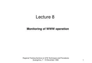
Lecture 8. Customer Integrated Circuits. ASIC. (F)PLD. FPGA. PAL. Gate Array. Full Custom. Std Cell. SoC. SoPC. CPLD. PLD. ASIC = Application Specific Integrated Circuit Gate Array = Prefabricated wafer with logic+added interconnections (metal layers). Vol > 10k

E N D
Lecture 8 Custom Designed Integrated Circuits
Customer Integrated Circuits ASIC (F)PLD FPGA PAL Gate Array Full Custom Std Cell SoC SoPC CPLD PLD ASIC= Application Specific Integrated Circuit Gate Array= Prefabricated wafer with logic+added interconnections (metal layers). Vol > 10k Standard Cell = Library with components (e.g. gates, multiplexors, flip-flops). Precompiled on transistor level. Vol >100k Full Custom = Transistor level design. Used for analog circuits. SoC = System on Chip. Processors and logic on chip. FPLD = Field Programmable Logic Device. FPGA = Field Programmable Gate Array. >1 milj gates! PLD = Programmable Logic Device CPLD = Complex PLD. <10k gates SoPC = System on Programmable Chip Custom Designed Integrated Circuits
ASIC Design Phases Design • From idea to synthesizable model • From synthesizable model masks Wafer fabrication • To check the fabricated chip • Slicing of wafer into separate chips wire bonding packaging Fabrication Testing Packaging Custom Designed Integrated Circuits
ASIC Design Phase Design Synthesis and Optimization Fabrication Netlist Validation Place & RouteSimulations Testing GDS-II tape Mask set(Photo masks) Packaging Custom Designed Integrated Circuits
ASIC Fabrication Phase Dia= 4”, 6”, 8”.. etcThickness = 0.5 mm Design Silocon wafers Fabrication Semiconductors fabrication Standard cell & Full custom Testing Metal layers inter- connections Only custom stage in Gate Array Packaging Custom Designed Integrated Circuits
ASIC Fabrication Phase Design Fabrication Test vectors Wafer tests(Probing of pads) Testing Test equipment Connection pads Packaging Chip Wafer Custom Designed Integrated Circuits
ASIC Fabrication Phase Design Scribing(Cutting wafers to chips) chip Fabrication Bonding e.g. wire bonding to lead frame Testing Plastic moulding or ceramic packaging Packagingand test Test of circuits Test vectors Custom Designed Integrated Circuits
n-MOS transistor basics Gate oxide Source Drain Gate Positive voltage on the gate will result in a channel of electrons below the gate oxide (inversion => majority carriers will be replaced with minority carriers). - - - - - - - - - - - - - - - - - - - - - - - - p+ n+ n+ Channel (minority carriers=e-) Custom Designed Integrated Circuits
p_MOS transistor basics Gate oxide Source Drain Gate Negative voltage (relative source) on the gate will result in a channel of holes below the gate oxide (inversion => majority carriers will be replaced with minority carriers). p+ n-well n+ p+ p+ + + + + + + + + + + + + + + + + + + + p+ p+ Custom Designed Integrated Circuits
ASIC Fabrication PhasesLithography Si - substrate Si-oxide Si - substrate Photo resist:Organic polymer. Positive photo resist:soluble after exposure with UV-light (shorter and shorter wavelengths required) photo resist Si - substrate UV -light Glass photo mask Si - substrate Si - substrate etching Custom Designed Integrated Circuits
SiO2 Si-substrate SiO2 Si-substrate n-channel MOSFET SiO2 Si-substrate Etching Doping(diffusion / Ion implantation) Si-substrate n+ n+ Poly silicon SiO2 metal connectors Thin oxide Si-substrate Si-substrate n+ n+ SiO2 Si-substrate Custom Designed Integrated Circuits
in out VDD VSS p+ p+ n+ n+ n+ n-well p+ CMOS inverter in Custom Designed Integrated Circuits
CMOS inverter Vout Vin Custom Designed Integrated Circuits
CMOS inverter Custom Designed Integrated Circuits
a & z b z a b CMOS circuits NAND gate P P N N Custom Designed Integrated Circuits
VLSI words • 0.25 micron process, 0.13 micron process, 0.09 micron process:smallest dimension in a transistor is 0.25 micro meter etc • Cu- layers. Copper is used for the metal layers => lower resistance in the signal wires. 9 metal layers is not unusual! • 6 inch wafer, 8 inch wafer: Diameter is 6 inches, 8 inches (newest). • NRE (Non Recurring Engineering costs. Includes e.g. mask set costs. NRE increases with new (smaller) technology Custom Designed Integrated Circuits
NRE cost evaluation • Typical cost for an ASIC in 0.18 m is $5 millions, in 0.13 m $10 millions. Future 0.45 m will cost more than $15 millions. • Only Asic’s in very high volumes possible (>100k, >1000k) • Possible solutions to ASIC cost problem: • “Structured ASIC”: Modern Gate Array (GA) with more complex building blocks than traditionally GA’s. • Converted FPGA to “Hardwired FPGA” => faster, cheaperhttp://www.altera.com/products/software/pld/products/q2/qts-index.html?xy=qts-gif Custom Designed Integrated Circuits
VHDL Test bench problem ARCHITECTURE behav OF tb_exempel IS component tt_buffer is port(rd: in std_logic; out_buffer: inout std_logic_vector(7 downto 0)); end component; signal rd: std_logic; signal out_buffer: std_logic_vector(7 downto 0); BEGIN u1: tt_buffer port map (rd,out_buffer); process begin rd<='1'; wait for 500 ns; rd<='0'; wait; end process; process begin wait for 1 us; out_buffer<="10101010"; wait; end process; END behav; - tb_exempel -- joal 2003-10-07 -- Abstract: To demonstrate how multiple drivers can be -- generated in a test bench and -- how to avoid problems with that LIBRARY ieee; USE ieee.std_logic_1164.ALL; USE ieee.std_logic_arith.ALL; -- *********************************************** LIBRARY ieee; USE ieee.std_logic_1164.ALL; USE ieee.std_logic_arith.ALL; ENTITY tb_exempel IS END tb_exempel ; Custom Designed Integrated Circuits
VHDL Test bench problem ARCHITECTURE behav OF tb_exempel IS component tt_buffer is port(rd: in std_logic; out_buffer: inout std_logic_vector(7 downto 0)); end component; signal rd: std_logic; signal out_buffer: std_logic_vector(7 downto 0); BEGIN u1: tt_buffer port map (rd,out_buffer); process begin rd<='1'; wait for 500 ns; rd<='0'; wait; end process; process begin -- out_buffer driver in this process must have a start value – otherwise ’U’ is used and can't be resolved!!!! out_buffer<="ZZZZZZZZ"; wait for 1 us; out_buffer<="10101010"; wait; end process; END behav; - tb_exempel -- joal 2003-10-07 -- Abstract: To demonstrate how multiple drivers can be -- generated in a test bench and -- how to avoid problems with that LIBRARY ieee; USE ieee.std_logic_1164.ALL; USE ieee.std_logic_arith.ALL; -- *********************************************** LIBRARY ieee; USE ieee.std_logic_1164.ALL; USE ieee.std_logic_arith.ALL; ENTITY tb_exempel IS END tb_exempel ; Custom Designed Integrated Circuits
VHDL Test bench problem Before code corrected rd out_buffer UUUUUUUU 10101010 After code corrected rd out_buffer 01010101 10101010 1 ms Custom Designed Integrated Circuits
IEEE 1076.1-1999 /VHDL-AMS, Analog modeling added http://www.eda.org/vhdl-ams/ ---------------------------------------------------------------------- -- The capacitor definition begins..... ---------------------------------------------------------------------- -- Schematic of the capacitor component: -- -- Ta1 o----||----o Tb1 -- ---------------------------------------------------------------------- LIBRARY DISCIPLINES; USE DISCIPLINES.ELECTROMAGNETIC_SYSTEM.ALL; ENTITY Capacitance IS GENERIC (val : REAL); PORT (TERMINAL p,m : ELECTRICAL); END; ARCHITECTURE behav OF Capacitance IS QUANTITY u_c ACROSS i_c THROUGH p TO m; BEGIN i_c==val * u_c'dot; END; Custom Designed Integrated Circuits
VHDL-AMS, Analog modeling added Custom Designed Integrated Circuits