Download
1 / 56
560 likes | 659 Vues
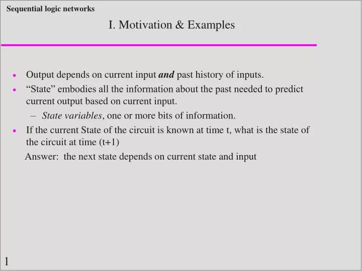
I. Motivation & Examples. Output depends on current input and past history of inputs. “State” embodies all the information about the past needed to predict current output based on current input. State variables , one or more bits of information.

E N D
I. Motivation & Examples • Output depends on current input and past history of inputs. • “State” embodies all the information about the past needed to predict current output based on current input. • State variables, one or more bits of information. • If the current State of the circuit is known at time t, what is the state of the circuit at time (t+1) Answer: the next state depends on current state and input
on u u u u u … 1 2 3 4 99 d d d d d I. Motivation & Examples Describing sequential circuit • State table • For each current-state, specify next-states as function of inputs • For each current-state, specify outputs as function of inputs • State diagram • Graphical version of state table Example 1: TV channel control • Let the channel # represent the state of the circuit • Input are up/down on the channel control u: up d: down
I. Motivation & Examples Example 2: A sequential process that inputs an n-bit binary string and outputs 1 if the string contains an even number of 1’s 1 (final output) 01111 SLN 0 (final output) 0111 SLN • What represents the state of the circuit? • Case1: • State as the number of 1’s read so far (possibly infinite # of states) • Case 2: Two states E and O • E (even): if the # of 1’s read so far is even • O (odd) if the # of 1’s read so far is odd
Input Output 1/0 E O 1/1 0/0 0/1 I. Motivation & Examples Example 2: State Diagram for Case 1 Input Output 1/0 1/1 1/0 1/1 1/0 1/1 … 0 1 2 3 4 2n 0/1 0/1 0/1 0/1 0/0 0/0 Example 2: State Diagram for Case 2
Input Output 1/0 E O 1/1 0/0 0/1 I. Motivation & Examples Example 2: State Diagram for Case 2 • Better design • Has less states
I. Motivation & Examples • Example 3: Discuss sequential n-bits comparator • Compare two n-bits numbers X=[Xn-1, …, X0], Y=[Yn-1, …, Y0] • Output 1 if X>Y • Use the basic 1-bit comparator designed in class Shift right ... Xn-1 Xn-2 Xn-3 X2 X1 X0 Operation controlled by a clock to decide: Xi Fi-1 .when to shift input data .when output Fi is stable 1-bit Comparator Ci Yi ... Yn-1 Yn-2 Yn-3 Y2 Y1 Y0 Fi Shift right
I. Motivation & Examples • Example 4: Discuss sequential n-bits adder • Add two n-bits numbers X=[Xn-1, …, X0], Y=[Yn-1, …, Y0] • Output S=X+Y where [Sn,Sn-1,…,S0] • Use the basic 1-bit adder with carry in and carry out Shift right ... Xn-1 Xn-2 Xn-3 X2 X1 X0 Operation controlled by a clock to decide: Xi Ci-1 .when to shift input data .when output are ready 1-bit Full adder Ci Yi ... Yn-1 Yn-2 Yn-3 Y2 Y1 Y0 Ci Shift right Shift right ... Sn Sn-1 Sn-2 S2 S1 S0
Clock signals II. General Representation • Sequential circuit are controlled by a clock signal • Very important with most sequential circuits • State variables change state at clock edge.
General diagram of sequential circuit II. General Representation • Sequential circuit are controlled by a clock signal • Very important with most sequential circuits • State variables change state at clock edge. Input Output i0 i1 … in o0 o1 … om SLN Current states Next states Feedback Memory components State variables: s0,s1, …sk
Some important questions II. General Representation • How to represent the states of a sequential circuit? • How to memorize the (current and next) states? • How to determine the next of the circuit? • How to determine the outputs • as a function F(state) of current state only? • as a function F(input,state) of both input and current state? • The concept of STATE is very important
Memory component II. General Representation • How do we represent the states? • Memory component are used as state variables • Goal: Memorize the current state of the circuit • How are memory components implemented? • Latch, Flip-flop are 1-bit memory component
Bistable element III. Basic memory component • The simplest sequential circuit • Two states • One state variable, say, Q (QN or Q_L the complement of Q) HIGH LOW LOW HIGH
Bistable element III. Basic memory component • The simplest sequential circuit • Two states • One state variable, say, Q LOW HIGH HIGH LOW
Bistable element: Analog analysis III. Basic memory component • Assume pure CMOS thresholds, 5V rail • Theoretical threshold center is 2.5 V
Bistable element: Analog analysis III. Basic memory component • Assume pure CMOS thresholds, 5V rail • Theoretical threshold center is 2.5 V 2.5 V 2.5 V 2.5 V 2.5 V
2.0 V 2.0 V Bistable element: Analog analysis III. Basic memory component • Assume pure CMOS thresholds, 5V rail • Theoretical threshold center is 2.5 V 2.5 V 4.8 V 2.51 V 2.5 V 0.0 V 2.5 V 0.0 V 4.8 V 5.0 V 2.5 V
Bistable element: summary II. General Representation • If (Q=0), then input to Not gate 2 is 0 ==> Output of Not gate 2 is 1 (Q_L =1) ==> The input of Not gate 1 is 1, so output of Not gate 1 is 0 ==> Stable output (Q=0) and (Q_L = 1) • If (Q=1), then input to Not gate 2 is 1 ==> Output of Not gate 2 is 0 (Q_L =0) ==> The input of Not gate 1 is 0, so output Not gate 1 is ==> Stable output (Q=1) and (Q_L = 0) 1 2
Contradiction!!!! S-R Latch…. III. Basic memory component • How to control it? • Screwdriver • Control inputs • S-R latch
S-R Latch…. III. Basic memory component Set operation: SR 00 ----> 10, set the device output to Q=1 regardless of current value of Q Reset operation: SR 00 ----> 01, set the device output to Q=0 regardless of current value of Q Hold operation: SR 10 ----> 00 or 01 ----> 00, Device output are the same as last output values • Only one input value changes • Possible input changes: • SR: 00 ---> 01 ---> 00 ---> 10 ---> 00 …. • Input SR = 11 is not allowed ( Both NOR gates output 0, i.e Q=Q’=0 )
S-R latch operation III. Basic memory component
Progation delay Minimum time to maintain signal at 1 S-R latch timing parameters III. Basic memory component • Propagation delay • Minimum pulse width
S-R latch with enable III. Basic memory component
Input Output i1 o1 in SLN om M1 . . . . . . . . . Mk Sequential network architecture (revisited) III. Basic memory component Components Mi are latches/Flip flops • Operation rules: • Memory components Mi must be in stable state before input changes • Only one input of the component Mi can change at a time
S R q Q Q=q 0 0 0 Hold 0 0 1 Q=0 0 1 0 Reset 0 1 1 Q= 1 1 0 0 Set 1 0 1 1 1 0 Not allowed 1 1 1 III. Basic memory component Charcteristics equation of S-R latch Definition: The characteristic equation specifies a flip-flop next state as a function of its current state and inputs Notation: Let q represent the current state of the flip-flop and Q its next Characteristics table 0 1 0 0 1 1 X X
Hold Reset Set Charcteristics table (other representation) III. Basic memory component Characteristics table S R Q q 0 0 Q=q 0 0 1 Q=0 1 1 0 Q= 1 X 1 1 Not allowed
Q SR 00 01 11 10 q 0 S R q Q X 1 Q=q 1 0 0 0 1 1 X 0 0 1 Q=0 0 1 0 0 1 1 Q= 1 1 0 0 Use K-map method to derive the characteristics equation: Q = S + R’q 1 0 1 1 1 0 1 1 1 III. Basic memory component Charcteristics equation of S-R latch Use the characteristics table to get an excitation map of the flip flop Characteristics table 0 1 0 0 1 1 X X
0 0 to hold current value q ---> Q S R 0 ---> 0 OR 0 X 0 1 to reset Q=0 0 ---> 1 1 0 0 0 to hold current value 1 ---> 0 0 1 1 ---> 1 X 0 OR 1 0 to set Q=1 III. Basic memory component Excitation table of SR flip flop The excitation table describes the input values of S and R that cause the corresponding transitions (q ---> Q) from current to next state Types of transitions: q --->Q 0 ---> 0 0 ---> 1 1 ---> 0 1 ---> 1 Excitation table of S R latch
J K q Q Q=q 0 0 0 Hold 0 0 1 Q=0 0 1 0 Reset 0 1 1 Q= 1 1 0 0 Set 1 0 1 1 1 0 Q = Q’ (Toggle) 1 1 1 III. Basic memory component JK Flip- Flop Recall: In SR flip flop, both input S, R cannot be 1 (SR=11) This restriction is removed in a JK flip flop. The behavior of the JK flip flop is as follows: Characteristics table 0 1 0 0 1 1 1 0
Hold Hold Reset Reset Set Set Charateristics of JK flip flop (other representation) III. Basic memory component Characteristics table J K Q q 0 0 Q =q 0 0 1 Q =0 1 1 0 Q = 1 q' 1 1 Q = q’ (Toggle) Characteristics table ( Clocked JK flip flop ) C J K Q q 1 0 0 Q =q 0 1 0 1 Q =0 1 1 1 0 Q = 1 q' 1 1 1 Q = q’ (Toggle) Disabled 0 x x
J K q Q Q=q 0 0 0 0 0 1 Q=0 0 1 0 0 1 1 Q= 1 1 0 0 Use K-map method to derive the characteristics equation: Q = Jq’ + Kq 1 0 1 1 1 0 Q = Q’ 1 1 1 Charcteristics equation of Jk Flip flop III. Basic memory component Use the characteristics table to get an excitation map of the flip flop Characteristics table Q JK 0 00 01 11 10 1 q 0 0 0 1 1 0 0 1 1 1 1 0 0 1 1 0
0 0 to hold current value q ---> Q J K 0 ---> 0 OR 0 X 0 1 to reset Q=0 0 ---> 1 1 X 0 0 to hold current value 1 ---> 0 X 1 1 ---> 1 X 0 OR 1 0 to set Q=1 III. Basic memory component Excitation table of JK flip flop The excitation table describes the input values of S and R that cause the corresponding transitions (q ---> Q) from current to next state Types of transitions: q --->Q 0 ---> 0 0 ---> 1 1 ---> 0 1 ---> 1 Excitation table of JK flip flop
0 0 to hold current value q ---> Q J K 0 ---> 0 OR 0 X 0 1 to reset Q=0 0 ---> 1 1 X 0 0 to hold current value 1 ---> 0 X 1 1 ---> 1 X 0 OR 1 0 to set Q=1 III. Basic memory component Excitation table of JK flip flop The excitation table describes the input values of S and R that cause the corresponding transitions (q ---> Q) from current to next state Types of transitions: q --->Q 0 ---> 0 0 ---> 1 1 ---> 0 1 ---> 1 Excitation table of JK flip flop
JK Flip flop Symbols III. Basic memory component J Q J Q K Q K QN Clocked JK Flip flop J Q J Q CK CK K QN K QN
D Flip- flop ( Delay flip flop) III. Basic memory component This flip flop has only one control input. The D flip flop simply retains its input between clock pulses Characteristics table D q Q 0 0 0 0 0 1 Q=d 1 1 0 1 1 1 Characteristics table ( Clocked D flip flop ) C D Q 1 0 0 Q=d 1 1 1 0 x Disabled
Characteristics equation: Q = D Charcteristics equation of D Flip flop III. Basic memory component Use the characteristics table to get an excitation map of the flip flop Characteristics table D q Q 0 0 0 1 0 1 0 1 0 1 1 1
D Flip flop Symbols III. Basic memory component D Q D Q Q QN Clocked JK Flip flop D Q D Q CK CK QN QN
D latch III. Basic memory component
D-latch operation III. Basic memory component
D-latch timing parameters III. Basic memory component • Propagation delay (from C or D) • Setup time (D before C edge) • Hold time (D after C edge)
Edge-triggered D flip-flop behavior III. Basic memory component
D flip-flop timing parameters III. Basic memory component • Propagation delay (from CLK) • Setup time (D before CLK) • Hold time (D after CLK)
IV. Counters Definitions • A counter is a sequential-circuit that generates a predetermined number sequence over and over again • A counter can be used as • a digital clock • special sequence generator • program counter • pulse counter
0 1 2 3 4 5 6 0 1 2 3 4 5 6 7 8 9 00 01 11 10 0000 0001 0011 0010 0110 0100 IV. Counters Examples
IV. Counters Types of counters • Counters are often implemented by Flip flops. They are • synchronous if all flip flops are clocked by the same signal • ripple (asynchronous) individual flip flop are clocked at different times • Counters may be classified by other characteristics: • mod N counter or divide-by- N counter, if counter has N distinct states (State = a number of the counted sequence) • by the number of fli flops in the counter: n bit counter • Other types of counter: • binary up (or down) counter : successive states represent an increasing binary count 00 --> 01 --> 10 --> 11 --> 00 …….. • gray code binary counter 00 --> 01 ---> 11 ---> 10 ---> 00
00 01 10 11 IV. Counters Intuitive Design of a counter • Problem Statement Design a sequential device to generate the sequence 0, 1, 2, 3 over and over again • There are 4 distinct states (divide-by-4) counter • Encode the four states as follows; 0 encoded by 00 1 encoded by 01 2 encoded by 10 3 encoded by 11 • Represent each binary bit of a code by a flip flop (in this example, let us use JK flip flops to design the counter)
00 00 01 01 10 10 11 11 Flip flop 1 00 Flip flop 0 IV. Counters Intuitive Design of a counter • Flip flop 0 changes state at every clock pulse • Flip flop 1 changes states every two clock pulses State transition flip flop 0 State transition flip flop 0
S0 S1 1 J Q J Q CK CK 1 K QN K QN EN IV. Counters Intuitive Design of a counter Design using JK flip flops for states 0 and 1 of the counter S1S0 : 00 --> 01 --> 10 --> 11 --> 00 …….
IV. Counters Intuitive Design of a 4 bit binary counter Design using JK flip flops S3S2S1S0 : 0000 --> 0001 --> 0010 --> 0011 --> 0100 --> 0101 … --> 1111 --> 0000 • There are 16 states • design requires four flip flops • Synchronous design, all flip flops clocked by the same signal • S0 Changes state (toggles) every clock pulse • S1 Changes state (toggles) when S0 = 1 • S2 Changes state (toggles) when S1=1 and S0 = 1 • S3 Changes state (toggles) when S2=1, S1=1 and S0=1