Download
1 / 28
280 likes | 481 Vues
Module 4: Metrics & Methodology Topic 4: Recovered Clock Timing. OGI EE564 Howard Heck. Where Are We? . Introduction Transmission Line Basics Analysis Tools Metrics & Methodology Synchronous Timing Signal Quality Source Synchronous Timing Recovered Clock Timing Design Methodology

E N D
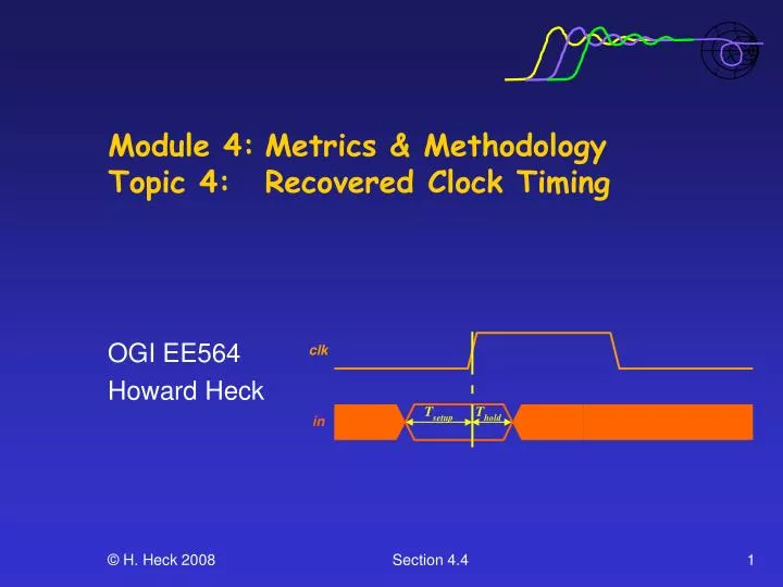
Module 4: Metrics & MethodologyTopic 4: Recovered Clock Timing OGI EE564 Howard Heck Section 4.4
Where Are We? • Introduction • Transmission Line Basics • Analysis Tools • Metrics & Methodology • Synchronous Timing • Signal Quality • Source Synchronous Timing • Recovered Clock Timing • Design Methodology • Advanced Transmission Lines • Multi-Gb/s Signaling • Special Topics Section 4.4
Why Another Clocking Scheme? 2 Problems of interest: • What do we do when we’re trying to communicate between devices that don’t have a “common clock?” • e.g. an external device? • Both devices will have clocks, but those clocks will not have a known phase relationship. We have to deal with it. • What do we do when we’re sending data at multi-GTs speeds, while low cost system clocks operate below 1 GHz? • In such cases, we typically do not send an explicit clock signal to the devices at all. • Instead, we “extract” the clock information from the data stream. Section 4.4
Contents • Goal • Timing Relationships & Equations • Example System & Operation • Summary Section 4.4
Goals • Our goal is to establish and maintain a desired phase relationship between DCLK and RCLK in order to ensure that we successfully transmit and receive data. • The phase relationship between the system clock inputs cannot be predetermined or directly controlled, so we must do it locally on each device. • We can also use the local adjustment circuitry to generate high frequency local clocks for controlling the data transfer. Section 4.4
Data-Clock Phase Relationship DCLK T CO Data @ A T f T flight Data @ B 90° RCLK • The receiver clock recovery circuitry attempts to center the receiver clock in the data eye. • i.e. maintain a 90 offset between B and RCLK. • Accounting for driver and interconnect delay, the desired phase relationship between DCLK and RCLK is: • Jitter on the driver, receiver, and interconnect, and frequency differences between will degrade the phase relationship (i.e. setup/hold margin) between B and RCLK. Section 4.4
Phase Relationship - Setup T ( DCLK) pushout DCLK T =T +T CO,max co co,pushout Data @ A T =T + T flight,max flight flight,pushout Data @ B RCLK 90° - (T + T ) flight,pushout CO,pushout T ( RCLK) - T (RCLK) - T (DCLK) pullin pullin pushout • Worst case setup case: • TCO & Tflight increase • DCLK pushes out • RCLK pulls in • The corresponding DCLK to RCLK relationship is shown below: • Tco,max and Tflight,max are taken over M cycles. They include ISI, crosstalk, SSO, etc. • Tpushout(DCLK) is the maximum pushout of the driver clock after M cycles w.r.t. to the edge at the 1st cycle. • Tpullin(RCLK) is the maximum pullin of the receiver clock after M cycles w.r.t. to the edge at the 1st cycle. Section 4.4
Phase Relationship - Hold T ( DCLK) pullin DCLK T = T - T CO,min CO CO,pullin Data @ A T = T - T flight,min flight flight,pullin Data @ B RCLK 90° - (T + T ) flight,pullin CO,pullin T ( RCLK,) - T (DCLK,) - T (RCLK) pushout pullin pushout • Worst case setup case: • TCO & Tflight decrease • DCLK pulls in • RCLKpushes out • The corresponding DCLK to RCLK relationship is shown below: • Tco,min and Tflight,min are taken over M cycles. They include ISI, crosstalk, SSO, etc. • Tpullin(DCLK) is the maximum pullin of the driver clock after M cycles w.r.t. to the edge at the 1st cycle. • Tpushout(RCLK) is the maximum pushout of the receiver clock after M cycles w.r.t. to the edge at the 1st cycle. Section 4.4
Setup & Hold Equations (Skipping the derivation) • Define Tx, Rx, and flight time jitter: • Tx jitter (DTTX,max) is maximum phase uncertainty of transmitted data including variation in the local clock. • Rx jitter (DTRX,max) is maximum phase uncertainty of received data including variation in the local clock. • Flight time jitter (DTlightmax) is maximum phase uncertainty of the interconnect flight time • All quantities are positive for setup, negative for hold • Keeps with previous conventions • Ideal phase relationship between data edge at the receiver input and RCLK. • Here are the simplified setup & hold equations: Section 4.4
Example Extracted Clock System • System clock (SCLK) is multiplied by N to produce higher frequency at C. • The local clock is phase aligned to the output of the loop filter, producing local clock, DCLK. • DCLK is divided by N , and the phase of D is compared to the system clock, SCLK, producing E. • Phase error is averaged over several clock cycles by the loop filter and fed back to the clock adjustment circuit (F). Section 4.4
Example Extracted Clock System (2) • The feedback loop described on the previous slide is designed to lock DCLK to an exact multiple of SCLK, providing a stable high frequency clock for the transmitter. • DCLK controls the latching of data to the transmitter (A). • The data bit travels down the line to the receiver (B). Section 4.4
Example Extracted Clock System (3) • Data at B is latched by RCLK , which has the same frequency as DCLK. RCLK may or may not have the same system clock source as DCLK. • The delay element shifts RCLK 90 out of phase from B to center the clock in the data bit, with adjustment by the phase comparator/filter/clock adjust loop. • Note that the loop time constant is several cycles, so it does not correct high frequency phase deviations. Section 4.4
Question • What requirement does the periodic clock adjustment place on the operation of a channel that uses an extracted clock? Section 4.4
References • S. Hall, G. Hall, and J. McCall, High Speed Digital System Design, John Wiley & Sons, Inc. (Wiley Interscience), 2000, 1st edition. • W. Dally and J. Poulton, Digital Systems Engineering, Cambridge University Press, 1998. • R. Poon, Computer Circuits Electrical Design, Prentice Hall, 1st edition, 1995. • H.B.Bakoglu, Circuits, Interconnections, and Packaging for VLSI, Addison Wesley, 1990. • H. Johnson and M. Graham, High Speed Digital Design: A Handbook of Black Magic, PTR Prentice Hall, 1993. • S. Dabral and T. Maloney, Basic ESD and I/O Design, John Wiley and Sons, New York, 1998. Section 4.4
Appendix: Extracted Clock Equation Derivation Section 4.4
Clock Drift • Assuming DCLK is updated every M cycles, the phase error quantifies how much the Mth DCLK edge deviates from the placement of the Mth RefCLK edge. • Deterministic noise is caused by sources such as power supply switching, temperature variation, bus noise, and spread spectrum clocking. • Gaussian noise is random, which noise, not correlated to any specific source, and will tend to average zero over time. Section 4.4
Clock Drift & Adjustment Hold Requirement Hold side margin • Variations in flight time and driver delay degrade the phase relationship, and therefore the setup/hold window. • Both clocks drift with time, and are adjusted periodically, depending on PLL bandwidth, clock extraction circuits, and Tco and Tflight variations. • Interconnect variations tend to be higher frequency, and are not compensated by the clock extraction circuits. Setup side Margin Setup Requirement Cycles(N) N=1 N=P N=2M N=M High Frequency Interconnect Noise Low frequency drift between Dclk and Rclk Section 4.4
Data Path Delay [8.3.4] Section 4.4
Clock Path Delay [8.3.5] Phase difference, TDf is: [8.3.6] Tferror is the phase error at calibration (N=1). Section 4.4
Setup Loop [8.3.7] Section 4.4
Setup Equation • Starting with the loop equation: [8.3.7] • Define the initial phase offset, Tf: [8.3.8] [8.3.9] • Simplify the loop equation: [8.3.10] Section 4.4
Setup Equation #2 • Define worst case transmitter and flight times for the setup case: • Simplify the loop equation: [8.3.11] Section 4.4
Setup Equation #3 • Define worst case transmitter, receiver, and flight time variation: Maximum data signal pushout w.r.t. refCLK over M cycles. [8.3.12] Minimum pull-in of RCLK w.r.t. refCLK over M cycles. [8.3.13] Maximum flight time variation over M cycles. [8.3.14] Minimum phase relationship between data edge at the receiver input and RCLK.. [8.3.15] • Rewrite the loop equation: [8.3.16] Section 4.4
Hold Loop [8.3.17] Section 4.4
Hold Equation • Starting with the loop equation: [8.3.17] [8.3.18] • Use the phase relationship: [8.3.19] • Recall: [8.3.9] Section 4.4
Hold Equation #2 • Work with the loop equation: [8.3.18] [8.3.20] Section 4.4
Hold Equation #3 [8.3.20] • Define: Minimum data signal pullin w.r.t. refCLK over M+1 cycles. [8.3.21] Maximum pushout of RCLK w.r.t. refCLK over M cycles. [8.3.22] Minimum flight time variation over M+1 cycles. [8.3.23] Maximum phase relationship between data edge at the receiver input and RCLK.. [8.3.24] Section 4.4
Hold Equation #4 • Finally: [8.3.25] Section 4.4