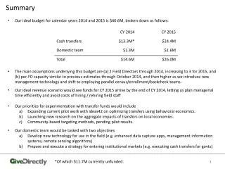
Download
1 / 21
210 likes | 214 Vues
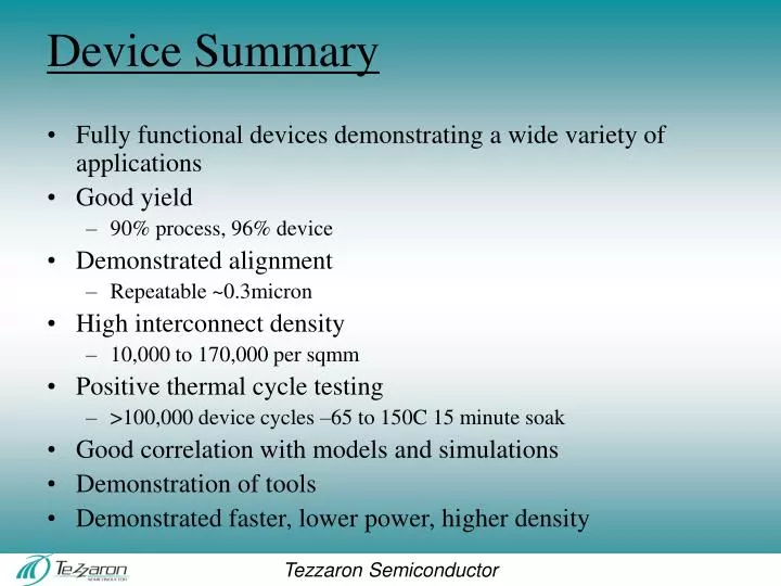
Fully functional devices demonstrating a wide variety of applications with good yield and high interconnect density. Demonstrated alignment and repeatable performance. Positive thermal cycle testing and good correlation with models and simulations. Demonstration of tools for faster, lower power, and higher density devices.

E N D
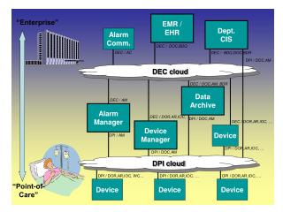
Device Summary • Fully functional devices demonstrating a wide variety of applications • Good yield • 90% process, 96% device • Demonstrated alignment • Repeatable ~0.3micron • High interconnect density • 10,000 to 170,000 per sqmm • Positive thermal cycle testing • >100,000 device cycles –65 to 150C 15 minute soak • Good correlation with models and simulations • Demonstration of tools • Demonstrated faster, lower power, higher density
Wafer to Wafer - Best Fit • Memory • DRAM • PCRAM, FERAM, MRAM • FPGA • Sensors • Processors • Short wires • Heat, heat, heat
Parameters • 10um Z dimension increments • 5-15um thickness • Low R • Moderate C • Repair & Redundancy • It’s still per sqmm! • Pitch • 0.5um limit • How many layers? • 2 to 5, current horizon
HEAT!!! • Modeling • What modeling, more data, more testing required • What we know…. • 32W/sqmm, Structurally sound • <5W easy rules • ~15W/100sqmm cliff • >150W possible • >500W liquid cooling
Even with innovations like DDR II* and QDR,* inadequate memory speed – the so-called “Memory Wall” – is still the primary obstacle to system performance;[i] it undermines most of the speed improvements of today’s processors.[ii] In spite of gains in bus speed, high memory latency causes processors to wait for data; 2003 statistics show that individual processors in high-performance systems and servers spend 65-95% of their time[iii] idly waiting for either memory or I/O. * Graph: J. Dongarra, U. of Tennessee • [i]N.R. Mahapatra and B. Venkatrao, “The Processor-Memory Bottleneck: Problems and Solutions” Association for Applied Computing Crossroads 5 no. 3 (1999) [e-journal]. • [ii]Anthony Cataldo, “MPU designers target memory to battle bottlenecks” EETimes, 19 October 2001 • [iii]Sally McKee, “Perspectives on The Memory Wall Problem” accessed online Sept. 2003 at http://www.lanl.gov/orgs/ccn/salishan2003/pdf/mckee.pdf. • Jack Dongarra, “Getting the Performance out of High Performance Computing” accessed online Sept. 2003 at http://www.nersc.gov/conferences/SciDAC2003/Presentations/Dongarra.pdf
Commodity Memory … FLAT!
A Poster Child for the Productivity Crisis Sparse Matrix Operations Particle Physics, Weapons Dev. 5.9% efficiency I/O BW to Processing Ratio Radar, Sonar, Imaging Sensors 12% efficiency Finite Element Analysis Weather & Ocean Forecasting 7.1% efficiency Memory Intensive Calculations Cryptanalysis < 3.0% efficiency Large Matrix Manipulation Engineering Design of Complex Structures 8.4% efficiency ASCI Q PC’s are 15 to 25% Efficient
Linear! When Processor Limited Comparable
3 Log! When Memory Limited 500 X 0.006
Where Does the Bandwidth Go? • When Costs are Grouped by Bandwidth, Memory Bandwidth is 80% of the Cost of a Cray X1 Class Machine
OK, access to main memory is glacial Solution: On Chip Cache
Cache THE Driver of Processor Die Area $4227 $1980 $TBD 90 nm 130 nm
The Good The Ugly The Bad
On Chip / Off Chip Power Operation Energy 32-bit ALU operation 5 pJ 32-bit register read 10 pJ Read 32 bits from 8K RAM 50 pJ Move 32 bits across 10mm chip 100 pJ Move 32 bits off chip 1300 to 1900 pJ Calculations using a 130nm process operating at a core voltage of 1.2V (Source: Bill Dally, Stanford) Prefetch/Cache Overhead and Off Chip Memory Access are key Power Issues
3D Heterogeneous Integration BEFORE Intel Photo used as proxy Only Memory Directly Compatible with Logic (virtually no choice!) Rendering of 3D IC Maps to logic only die Maps to memory die array AFTER: 3D IC 14x increase in memory density 4X Logic Cost Reduction 29x 100x memory cost reduction (choice!)
Octopus L3 Cache DRAM • 1Gb-4Gb • Down to 5ns, latency • 1GHz Max clock rate • Minimum Timing - tRCD=1, tCYC=4, tPRE=0, tCL=2 • Programmable 8 port by 256 bit architecture • Programmable burst length 4 to 256 • Programmable port width 32 to 256 bits • Exposed or hidden refresh options • DDR 2000MT Max • >200GB/s sustained, closed page mode, BL=4, bandwidth • 512GB/s peak bandwidth • >25TB/s peak on-board transfer rate • 1.0V to 1.7V I/O • 1.4V to 1.6V Core • Internally ECC protected, Dynamic self-repair • 115C die full function operating temperature • 65 sqmm die footprint