Download
1 / 37
490 likes | 1.38k Vues
Scanning Probe Microscopy. Alexander Couzis ChE5535. SPM Techniques. Scanning probe microscopes (SPMs) are a family of instruments used for studying surface properties of materials from the atomic to the micron level. All SPMs contain the components illustrated. Scanning Tunneling Microscopy.

E N D
Scanning Probe Microscopy Alexander Couzis ChE5535
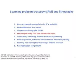
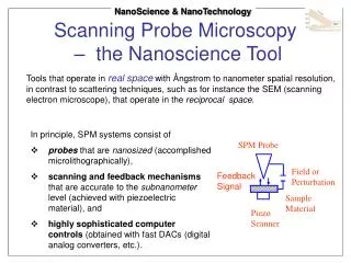
SPM Techniques Scanning probe microscopes (SPMs) are a family of instruments used for studying surface properties of materials from the atomic to the micron level. All SPMs contain the components illustrated
Scanning Tunneling Microscopy • The scanning tunneling microscope (STM) is the ancestor of all scanning probe microscopes. It was invented in 1981 by Gerd Binnig and Heinrich Rohrer at IBM Zurich. Five years later they were awarded the Nobel prize in physics for its invention. The STM was the first instrument to generate real-space images of surfaces with atomic resolution. • STMs use a sharpened, conducting tip with a bias voltage applied between the tip and the sample. When the tip is brought within about 10Å of the sample, electrons from the sample begin to "tunnel" through the 10Å gap into the tip or vice versa, depending upon the sign of the bias voltage. The resulting tunneling current varies with tip-to-sample spacing, and it is the signal used to create an STM image. For tunneling to take place, both the sample and the tip must be conductors or semiconductors. STMs cannot image insulating materials.
Modes of Operation for STM constant-height constant-current
STM • In constant-height mode, the tip travels in a horizontal plane above the sample and the tunneling current varies depending on topography and the local surface electronic properties of the sample. The tunneling current measured at each location on the sample surface constitute the data set, the topographic image. • In constant-current mode, STMs use feedback to keep the tunneling current constant by adjusting the height of the scanner at each measurement point. For example, when the system detects an increase in tunneling current, it adjusts the voltage applied to the piezoelectric scanner to increase the distance between the tip and the sample. In constant-current mode, the motion of the scanner constitutes the data set. If the system keeps the tunneling current constant to within a few percent, the tip-to-sample distance will be constant to within a few hundredths of an angstrom.
STM • Each mode has advantages and disadvantages. Constant-height mode is faster because the system doesn't have to move the scanner up and down, but it provides useful information only for relatively smooth surfaces. Constant-current mode can measure irregular surfaces with high precision, but the measurement takes more time. • As a first approximation, an image of the tunneling current maps the topography of the sample. More accurately, the tunneling current corresponds to the electronic density of states at the surface. STMs actually sense the number of filled or unfilled electron states near the Fermi surface, within an energy range determined by the bias voltage. Rather than measuring physical topography, it measures a surface of constant tunneling probability. • From a pessimist's viewpoint, the sensitivity of STMs to local electronic structure can cause trouble if you are interested in mapping topography. For example, if an area of the sample has oxidized, the tunneling current will drop precipitously when the tip encounters that area. In constant-current mode, the STM will instruct the tip to move closer to maintain the set tunneling current. The result may be that the tip digs a hole in the surface. • From an optimist's viewpoint, however, the sensitivity of STMs to electronic structure can be a tremendous advantage. Other techniques for obtaining information about the electronic properties of a sample detect and average the data originating from a relatively large area, a few microns to a few millimeters across. STMs can be used as surface analysis tools that probe the electronic properties of the sample surface with atomic resolution.
STM Image Showing Single-atom Defect in Iodine Adsorbate Lattice on Platinum. 2.5nm Scan
Atomic Force Microscopy • The atomic force microscope (AFM) probes the surface of a sample with a sharp tip, a couple of microns long and often less than 100Å in diameter. The tip is located at the free end of a cantilever that is 100 to 200µm long. Forces between the tip and the sample surface cause the cantilever to bend, or deflect. A detector measures the cantilever deflection as the tip is scanned over the sample, or the sample is scanned under the tip. The measured cantilever deflections allow a computer to generate a map of surface topography. AFMs can be used to study insulators and semiconductors as well as electrical conductors. • Several forces typically contribute to the deflection of an AFM cantilever. The force most commonly associated with atomic force microscopy is an interatomic force called the van der Waals force. The dependence of the van der Waals force upon the distance between the tip and the sample is shown in Figure 1-4.
AFM Two distance regimes are labeled: 1) the contact regime; 2) the non-contact regime. In the contact regime, the cantilever is held less than a few angstroms from the sample surface, and the interatomic force between the cantilever and the sample is repulsive. In the non-contact regime, the cantilever is held on the order of tens to hundreds of angstroms from the sample surface, and the interatomic force between the cantilever and sample is attractive (largely a result of the long-range van der Waals interactions).
AFM • At the right side of the curve the atoms are separated by a large distance. As the atoms are gradually brought together, they first weakly attract each other. This attraction increases until the atoms are so close together that their electron clouds begin to repel each other electrostatically. This electrostatic repulsion progressively weakens the attractive force as the interatomic separation continues to decrease. The force goes to zero when the distance between the atoms reaches a couple of angstroms, about the length of a chemical bond. • When the total van der Waals force becomes positive (repulsive), the atoms are in contact. The slope of the van der Waals curve is very steep in the repulsive or contact regime. As a result, the repulsive van der Waals force balances almost any force that attempts to push the atoms closer together. In AFM this means that when the cantilever pushes the tip against the sample, the cantilever bends rather than forcing the tip atoms closer to the sample atoms. Even if you design a very stiff cantilever to exert large forces on the sample, the interatomic separation between the tip and sample atoms is unlikely to decrease much.
AFM • In addition to the repulsive van der Waals force described above, two other forces are generally present during contact AFM operation: • A capillary force exerted by the thin water layer often present in an ambient environmen • The force exerted by the cantilever itself. • The capillary force arises when water wicks its way around the tip, applying a strong attractive force (about 10-8N) that holds the tip in contact with the surface. • The magnitude of the capillary force depends upon the tip-to-sample separation. • The force exerted by the cantilever is like the force of a compressed spring. • The magnitude and sign (repulsive or attractive) of the cantilever force depends upon the deflection of the cantilever and upon its spring constant.
AFM • As long as the tip is in contact with the sample, the capillary force should be constant because the distance between the tip and the sample is virtually incompressible. It is also assumed that the water layer is reasonably homogeneous. • The variable force in contact AFM is the force exerted by the cantilever. The total force that the tip exerts on the sample is the sum of the capillary plus cantilever forces, and must be balanced by the repulsive van der Waals force for contact AFM. • The magnitude of the total force exerted on the sample varies from 10-8 (with the cantilever pulling away from the sample almost as hard as the water is pulling down the tip), to the more typical operating range of 10-7to 10-6N.
Laser Diode Mirror Photodiodes Cantilever and Tip Feedback Image X-Y-P PiezoScanner AFM Operation Most AFMs currently on the market detect the position of the cantilever with optical techniques. In the most common scheme, a laser beam bounces off the back of the cantilever onto a position-sensitive photodetector (PSPD). As the cantilever bends, the position of the laser beam on the detector shifts. The PSPD itself can measure displacements of light as small as 10Å. The ratio of the path length between the cantilever and the detector to the length of the cantilever itself produces a mechanical amplification. As a result, the system can detect sub-angstrom vertical movement of the cantilever tip.
AFM Operation In constant-height mode, the spatial variation of the cantilever deflection can be used directly to generate the topographic data set because the height of the scanner is fixed as it scans. Constant-height mode is often used for taking atomic-scale images of atomically flat surfaces, where the cantilever deflections and thus variations in applied force are small. Constant-height mode is also essential for recording real-time images of changing surfaces, where high scan speed is essential. In constant-force mode, the deflection of the cantilever can be used as input to a feedback circuit that moves the scanner up and down in z, responding to the topography by keeping the cantilever deflection constant. In this case, the image is generated from the scanner's motion. With the cantilever deflection held constant, the total force applied to the sample is constant. In constant-force mode, the speed of scanning is limited by the response time of the feedback circuit, but the total force exerted on the sample by the tip is well controlled. Constant-force mode is generally preferred for most applications.
Non-Contact AFM Non-contact AFM (NC-AFM) is one of several vibrating cantilever techniques in which an AFM cantilever is vibrated near the surface of a sample. The spacing between the tip and the sample for NC-AFM is on the order of tens to hundreds of angstroms. NC-AFM is desirable because it provides a means for measuring sample topography with little or no contact between the tip and the sample. Like contact AFM, non-contact AFM can be used to measure the topography of insulators and semiconductors as well as electrical conductors. The total force between the tip and the sample in the non-contact regime is very low, generally about 10-12N. This low force is advantageous for studying soft or elastic samples. A further advantage is that samples like silicon wafers are not contaminated through contact with the tip.
Lateral Force Microscopy Lateral force microscopy (LFM) measures lateral deflections (twisting) of the cantilever that arise from forces on the cantilever parallel to the plane of the sample surface. LFM studies are useful for imaging variations in surface friction that can arise from inhomogeneity in surface material, and also for obtaining edge-enhanced images of any surface.
Lateral Force Microscopy Lateral deflections of the cantilever usually arise from two sources: changes in surface friction and changes in slope. In the first case, the tip may experience greater friction as it traverses some areas, causing the cantilever to twist more strongly. In the second case, the cantilever may twist when it encounters a steep slope. To separate one effect from the other, LFM andAFM images should be collected simultaneously.
Lateral Force Microscopy • LFM uses a position-sensitive photodetector to detect the deflection of the cantilever, just as for AFM. The difference is that for LFM, the PSPD also senses the cantilever's twist, or lateral deflection. • AFM uses a "bi-cell" PSPD, divided into two halves, A and B. • LFM requires a "quad-cell" PSPD, divided into four quadrants, A through D. By adding the signals from the A and C quadrants, and comparing the result to the sum fromthe B and D quadrants, the quad-cell can also sense the lateral component of the cantilever's deflection. A properly engineered system can generate both AFM and LFM data simultaneously.
Force Modulation Microscopy In FMM mode, the AFM tip is scanned in contact with the sample, and the z feedback loop maintains a constant cantilever deflection (as for constant-force mode AFM). In addition, a periodic signal is applied to either the tip or the sample. The amplitude of cantilever modulation that results from this applied signal varies according to the elastic properties of the sample
Force Modularion Microscopy The system generates a force modulation image, which is a map of the sample's elastic properties, from the changes in the amplitude of cantilever modulation. The frequency of the applied signal is on the order of hundreds of kilohertz, which is faster than the z feedback loop is set up to track. Thus, topographic information can be separated from local variations in the sample's elastic properties, and the two types of images can be collected simultaneously. topographic contact-AFM image (left) and an FMM image (right) of a carbon fiber/polymer composite
Phase Detection Microscopy Phase detection refers to the monitoring of the phase lag between the signal that drives the cantilever to oscillate and the cantilever oscillation output signal. Changes in the phase lag reflect changes in the mechanical properties of the sample surface.
Phase Detection Microscopy Non-contact AFM image (left) and PDM image (right) of an adhesive label,collected simultaneously. Field of view 3µm.
Electrostatic Force Microscopy Electrostatic force microscopy (EFM) applies a voltage between the tip and the sample while the cantilever hovers above the surface, not touching it. The cantilever deflects when it scans over static charges. EFM maps locally charged domains on the sample surface, similar to how MFM plots the magnetic domains of the sample surface. The magnitude of the deflection, proportional to the charge density, can be measured with the standard beam-bounce system. EFM is used to study the spatial variation of surface charge carrier density. For instance, EFM can map the electrostatic fields of a electronic circuit as the device is turned on and off. This technique is known as "voltage probing" and is a valuable tool for testing live microprocessor chips at the sub-micron scale.
Nanolithography Normally an SPM is used to image a surface without damaging it in any way. However, either an AFM or STM can be used to modify the surface deliberately, by applying either excessive force with an AFM, or high-field pulses with an STM. Not only scientific literature, but also newspapers and magazines have shown examples of surfaces that have been modified atom by atom. This techniqueis known as nanolithography. Photoresistive surface that has been modified using this technique.
10 m 10 m Mechanism of Silane Monolayer Formation from a Non-Competitive Solvent Surface Diffusion and Aggregation into “fractal-like” islands (primary growth) 10nm 5 nm 0 nm Surface Topography Image Friction Image
10nm 5 nm 0 nm Mechanism of Silane Monolayer Formation from a Non-Competitive Solvent Continued Adsorption Onto Bare Substrate Areas Leading to Full Coverage (secondary growth) HEIGHT SCALE 10 m Further Adsorption onto the surface leading to monolayer completion (dense packing) Such Growth also observed by Bierbaum et al(1995);Davidovitis et al(1996)
OTS Adsorption on Hydrated Substrate 10m 10nm 5 nm 0 nm HEIGHT SCALE HEIGHT FRICTION HEIGHT FRICTION IMAGE SIZE : 10m x 10m DEPOSITION TIME :1 sec DEPOSITION TIME : 5 sec OTS CONC. IN SOLUTION 2.06mM HEIGHT FRICTION HEIGHT FRICTION DEPOSITION TIME : 15 sec DEPOSITION TIME : 45 sec HEIGHT DEPOSITION TIME : 2 MIN
Mechanism of Silane Monolayer Formation from a Non-Competitive Solvent Continued Adsorption Onto Bare Substrate Areas Leading to Full Coverage Further Adsorption onto the surface leading to monolayer completion (dense packing)
10 m Effect of Surface Dehydration on OTS Deposition • Substrate Treated Under Different Conditions • Same Solvent and Deposition time (30sec) 10nm 5 nm 0 nm 57 56 58 Hydrated Substrate Substrate Dehydrated partially(100oC) Dehydrated Substrate (150oC)
In-situ Study of OTS Adsorption 10 m 10 m 10nm 5 nm 0 nm Blank solvents were passed over the substrate before OTS solution No solvents were passed over the substrate before OTS solution