Download
1 / 17

E N D
Thyristors Why Thyristors?
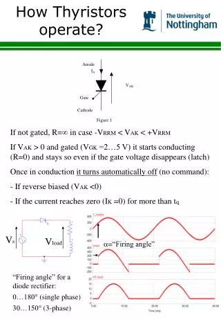
Silicon-controlled rectifier (SCR) “ or thyristor” is a three-terminal solid state device used to control large current to a load in one direction. It acts like a solid state switch because load current flows through its anode-cathode circuit. As shown in the figure, when a trigger current is applied at the gate terminal, the SCR is turned on thus allowing the current to flow from anode to cathode terminal. • SCR is on for a certain percentage of AC cycle and is off state for the remainder of the time. An SCR varies load current by varying the point in the positive half cycle of AC input when the current is applied at the gate terminal. • If the SCR is turned on immediately, then the load will receive current for nearly half of the cycle(180˚C). • SCR can be turned on in only positive half cycle. Figure 5–2 Circuit relationship among the voltage supply, an SCR, and the load.
iT On state voltage drop VTM On-state characteristic (Forward conduction) Latching current IL IG3 > IG2 > IG1 > IG0 Holding current IH vt Reverse breakdown voltage Forward blocking state characteristic IDRM at VDRM Off-state characteristic (Reverse blocking) Forward breakdown voltage • An SCR acts very much like a switch. When it is turned ON acts like a closed switch. When it is turned OFF, then it acts like an open switch. Because it is a Solid state device, the switching action is very fast.Elecetrical characteristics of SCR are shown in the figure below • TURN-ON CHARACTERISTICS • During the off state very current IDRM flows through the SCR but forward voltage VDRM is very high. • But when the gate current is applied, the forward voltage drops quickly to VTM and the current rises quickly to the holding current, IH . SCR is now in the on state. SCR ELECTRICL CHARACTERISTICS IT, IH, IGT, VTM , IL ? See the definitions in your textbook on page#219
Requirements to turn-on a thyristor:SCR’s breakdown voltage should never be exceeded because the SCR goes into conduction even when a gate current is not applied. It remain turn on even if the breakdown voltage is reduced.1. The thyristor must be forward biased (VAK > 0) AND2. There must be sufficient trigger current into the gate through the gate-cathode junction Requirements to turn-off a thyristor:1. The main terminal IT current must be below the holding current IH (IT < IH) 2. The thyristor is reversed biased .
Figure 5–3Ideal waveforms of SCR main terminal voltage (VAK) and load voltage: (a) for a firing delay angle of about 60, conduction angle of 120, (b) for a firing delay angle of about 135, conduction angle of 45.Firing angle delay is defined as number of degrees that the SCR is off before it turns on whereas the conduction angle is number of degrees that the SCR is on.
TYPICAL GATE TRIGGERING CIRCUITS • Resistive Circuit • Supply is AC (Sinusoidal) in Figure 5-6. • When SW is OPEN, the SCR can never turn on. The load therefore is deenergized. • When SW is CLOSED, there will be a current into the gate G of the SCR. Figure 5–6Very simple triggering circuit for an SCR.
The variable Resistance R2 will control the firing delay angle. • If R2 is low, IG will be sufficient to fire the SCR when the supply voltage is low (early firing, or delay angle is small). And Vice versa. • R1 is to maintain a fixed value of gate resistance when R2 is set to Zero. • Once the SCR is fired, all the load current will pass through it since it is a closed switch and there will be no gate current. The waveform of the load voltage will be similar to that in Figure 5-3.
The disadvantage of this circuit, is that the maximum firing delay angle is 90o only. This fact is shown in figure 5-7. If the supply voltage is DC, the SCR will remain ON until the supply is removed. One of the application of this simple circuit is in alarm systems. Figure 5–7Ideal waveforms of SCR main terminal voltage and gate current. The dashed line represents the gate current necessary to fire the SCR (IGT). (a) Gate current is low, resulting in a firing delay angle of about 90. (b) Gate current is greater, resulting in a firing delay angle of nearly 0.
2. Capacitor Triggering Circuit Figure 5–8SCR gate control circuit which is an improvement on the circuit of Fig. 5–6. The capacitor provides a greater range of adjustment of the firing delay angle. Figure 5-8 is an improvement on the circuit of Fig. 5–6 where a capacitor is added at the bottom of the gate lead resistance. The capacitor will guarantee the possibility of firing delay angle to be beyond 90O. For the negative half-cycle of the supply, the capacitor will charge in the reverse direction (top plate negative and the bottom plate positive).
For the positive half-cycle, the capacitor takes time to fully discharge and then charge in the positive direction (top plate positive and the bottom plate negative). • This will delay the current from flowing to the gate until the capacitor is charged higher than +0.6V. • The delay will depend on the value of R2. The bigger the value of R2 the slower the charging and the bigger the firing delay angle.
Figure 5-9 (a) shows a triggering circuit similar in operation to the previous one. The insertion of R3 requires the capacitor to charge higher than 0.6V to trigger the SCR. So the triggering is further delayed. In figure 5-9 (b), the firing is further delayed by the insertion of capacitor C2. Instead of immediately fire the SCR once the VC1 is enough to overcome the R3 drop, it will be used to charge C2 and only after C2 is charged higher than 0.6V IG will flow into the gate. Figure 5–9Improved SCR gate control circuits. Either one of these circuits provides a greater range of adjustment of the firing delay angle than the circuit of Fig. 5–8.
For given capacitor values (usually 0.01-1µF), the minimum firing delay angle is set by fixed resistor R1and R3 and the maximum delay angle is set by the size of the variable resistor R2 • Practically, (R1+R2)*C1 and R3*C2 should fall in the range of 1-30ms for a 60Hz supply. • Two problems are associated with the previous triggering circuits: • Temperature dependency. • Inconsistent firing behavior between SCRs of the same type.
3.Using a Breakover Device in the Gate Lead To overcome these problems a breakover device (e.g. four layer diode) is used as shown in figure 5-10. This device has certain breakover voltage point, if it is reached by VC it will act as a closed switch and allow the current to flow into the gate and hence firing the SCR, otherwise it will remain open. This device is relatively temperature-independent, and the breakover voltage can be held constant from one SCR to another, therefore the imperfection of the SCRs are of no importance. Figure 4–10SCR gate control circuit using a four-layer diode (or any breakover device). The four-layer diode provides consistency of triggering behavior and reduces the temperature dependence of the circuit.
SCRs in DC Circuits • When an SCR used in DC circuit the automatic turn-OFF does not occur, because the supply voltage does not pass thru Zero. • To off the SCR either disconnect the DC supply (which is not practical) or • Connect a temporary (for few µs) short circuit from the anode to the cathode of the SCR as shown in Figure 5-14(a).or by • Reverse-biasing the SCR as shown in Figure 5-14 (b). Figure 5–14SCR commutation circuits. (a) The transistor switch shorts out the SCR, thereby turning it OFF. (b) The transistor switch puts a charged capacitor in parallel with the SCR for reverse-bias turn-OFF. Often another SCR is used in place of the transistor.
Application Circuits of SCRs See page 228-229 for the description of the operation of this circuit (full-wave rectifier). This circuit usually used to design a dc power supply; as the output waveform is dc and the input supply is AC. • 1. Unidirectional Full-Wave Control Figure 5–11(a) Full-wave rectified power control, using two SCRs and a center-tapped winding. (b) Supply voltage and load voltage waveforms. Both ac half cycles are being used to deliver power, but the load voltage has only one polarity (it is rectified).
Figure 5–12(a) Full-wave unrectified power control, using two SCRs. (b) The same circuit drawn another way. (c) Load voltage waveform. Both ac half cycles are being used to deliver power, and the load voltage is unrectified. SCR1 fired on during the positive half-cycle of the ac supply, while SCR2 is fired ON during the negative half-cycle. Hence the output (load) voltage is uncertified. This circuit is called sometimes AC controller. • 2. Bidirectional Full-Wave Control
Figure 4–13Full-wave bridge combined with an SCR to control both halves of the ac line. (a) With the load inserted in one of the ac lines leading to the bridge, the load voltage is unrectified, as in Fig. 5–12(c). (b) With the load inserted in series with the SCR itself, the load voltage is rectified, as in Fig. 5–11(b). In the positive half-cycle of the AC supply, diodes A and C are forward biased; if the SCR is fired ON the ac voltage will be applied to the load. For the negative half-cycle, diodes B and D are forward biased and if the SCR fires the ac voltage will be applied to the load. The load voltage waveform will be similar to that shown in Figure 5-12 (c) 3. Bridge Circuit containing an SCR