Download
1 / 14
140 likes | 388 Vues
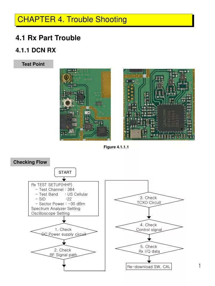
CHAPTER 4. Trouble Shooting. 4.1 Rx Part Trouble. 4.1.1 DCN RX. Test Point. Figure 4.1.1.1. Checking Flow. START. Rx TEST SETUP(HHP) - Test Channel : 384 - Test Band : US Cellular - SID :22 - Sector Power : -30 dBm Spectrum Analyzer Setting

E N D
CHAPTER 4. Trouble Shooting 4.1 Rx Part Trouble 4.1.1 DCN RX Test Point Figure 4.1.1.1 Checking Flow START Rx TEST SETUP(HHP) - Test Channel : 384 - Test Band : US Cellular - SID :22 - Sector Power : -30 dBm Spectrum Analyzer Setting Oscilloscope Setting 3. Check TCXO Circuit 4. Check Control signal 1. Check DC Power supply circuit 5. Check Rx I/Q data 2. Check RF Signal path Re-download SW, CAL
4.1.1.1 Checking DC Power supply Circuit Test Point Checking Flow +2.9V_Rx OK? Check Pin 5 of U105 NO The Problem may be Logic part Refer to Logic troubleshoot YES +2.6V_MSMP2 is OK? Check Pin 48 of U105 The Problem may be Logic part Refer to Logic troubleshoot NO YES U105. 5 DC Power supply Circuit is OK . See next Page to check RF Path. U105. 48 Figure 4.1.1.2 Circuit Diagram
4.1.1.2 Checking RF Signal path Test Point Checking Flow Check U101 Pin 2 Check if there is Any Major Difference ◆ Refer to Graph 4.1.1(a) U101. 2 U112. 2 Detected Signal? NO Changing U101 YES Check U112 Pin 2 Check if there is Any Major Difference ◆ Refer to Graph 4.1.1(a) Detected Signal? NO Check C101 Check L103 Check VR100 YES Check DP1 Pin 6 Check if there is Any Major Difference ◆ Refer to Graph 4.1.1(a) Changing U112 Check C1019Check C1022 Check L145 Detected Signal? NO YES DP1. 6 Check U105 Pin 33 Check if there is Any Major Difference ◆ Refer to Graph 4.1.1(b) Detected Signal? Changing DP 1 Check C175 & C173 & L118 NO YES F101. 1 Check F101 Pin 1 Check if there is Any Major Difference ◆ Refer to Graph 4.1.1(c) Changing U105 Check L125 & C188 NO Detected Signal? YES Check U105 Pin 23 Check U109 Pin 24 Check if there is Any Major Difference ◆ Refer to Graph 4.1.1(d) Detected Signal? Changing F101 Check C154 & C155 Check L108 & L114 NO U105. 23&24 YES U105. 33 RF Signal Path is OK . See next Page to check VCTCXO Circuit. Figure 4.1.1.3
Waveform Graph 4.1.1(b) Graph 4.1.1(a) Graph 4.1.1(c) Graph 4.1.1(d)
4.1.1.3 Checking TCXO Circuit Test Point Checking Flow(TCXO) TCXO Circuit is OK . YES Similar? Check X101 Pin 3 ◆ Refer to Graph 4.1.1(e) Check X101 Pin 4 No +2.8V OK? The Problem may be Logic part Refer to Logic troubleshoot NO YES Changing X101 Check R135 TCXO Circuit is OK . Check X101 Pin 3 ◆ Refer to Graph 4.1.1(e) X101. 3 X101. 4 YES Similar? NO Figure 4.1.1.4 SW Download Replace Board Waveform Circuit Diagram Graph 4.1.1(e)
4.1.1.4 Checking Control signal Test Point U105. 49 U105. 50 U105. 51 Figure 4.1.1.5 Checking Flow Check Pin 51(SBCK), Pin 49(SBST) Pin 50(SBDT) of U105. Check if there is Any Major Difference ◆ Refer to Graph 4.1.1(g.h) YES Control Signal is Ok See next Page to Check RX I&Q Data Similar? NO Download the SW YES Control Signal is Ok See next Page to Check RX I&Q Data Similar? Check Pin 51(SBCK), Pin 49(SBST) Pin 50(SBDT) of U105. Check if there is Any Major Difference ◆ Refer to Graph 4.1.1(g.h) NO Replace Board
Waveform SBCK SBCK SBDT SBST Graph 4.1.1(g) Graph 4.1.1(h) Circuit Diagram
4.1.2 PCS RX Test Point Figure 4.1.2.1 Checking Flow START Rx TEST SETUP(HHP) - Test Channel : 600 - Test Band : US PCS - SID :4182 - Sector Power : -30 dBm Spectrum Analyzer Setting Oscilloscope Setting 3. Check TCXO Circuit 4. Check Control signal 1. Check DC Power supply circuit 5. Check Rx I/Q data 2. Check RF Signal path Re-download SW, CAL
4.1.2.1 Checking DC Power supply Circuit Test Point Checking Flow +2.9V_Rx OK? Check Pin 5 of U105 NO The Problem may be Logic part Refer to Logic troubleshoot YES +2.6V_MSMP2 is OK? Check Pin 48 of U105 The Problem may be Logic part Refer to Logic troubleshoot NO U105. 5 YES U105. 48 DC Power supply Circuit is OK . See next Page to check RF Path. Figure 4.1.2.2 Circuit Diagram
4.1.2.2 Checking RF Signal path Test Point Checking Flow Check U101 Pin 2 Check if there is Any Major Difference ◆ Refer to Graph 4.1.2(a) U101. 2 U112. 2 Detected Signal? NO Changing U101 YES Check U112 Pin 2 Check if there is Any Major Difference ◆ Refer to Graph 4.1.2(a) Detected Signal? NO Check C101 Check L103 Check VR100 YES Check DP2 Pin 3 Check if there is Any Major Difference ◆ Refer to Graph 4.1.2(a) Changing U112 Check C1020 Check L144, C1021 Detected Signal? NO YES DP2. 3 Check U105 Pin 31 Check if there is Any Major Difference ◆ Refer to Graph 4.1.2(b) Detected Signal? Changing DP 2 Check C176 & L112 , C153 NO YES F104. 1 Check F104 Pin 1 Check if there is Any Major Difference ◆ Refer to Graph 4.1.2(c) Changing U105 Check C190Check C197, L129 NO Detected Signal? YES Check U105 Pin 25 Check U105 Pin 26 Check if there is Any Major Difference ◆ Refer to Graph 4.1.2(d) Detected Signal? Changing F104 Check C152 , C184 Check L105, L106 NO U105. 25&26 U105. 31 YES RF Signal Path is OK . See next Page to check VCTCXO Circuit. Figure 4.1.2.3
Waveform Graph 4.1.2(a) Graph 4.1.2(b) Graph 4.1.2(c) Graph 4.1.2(d)
4.1.2.3 Checking TCXO Circuit Test Point Checking Flow(TCXO) TCXO Circuit is OK . YES Similar? Check X101 Pin 3 ◆ Refer to Graph 4.1.1(e) Check X101 Pin 4 No +2.8V OK? The Problem may be Logic part Refer to Logic troubleshoot NO YES Changing X101 Check R135 TCXO Circuit is OK . Check X101 Pin 3 ◆ Refer to Graph 4.1.1(e) X101. 3 X101. 4 YES Similar? NO Figure 4.1.2.4 SW Download Replace Board Waveform Circuit Diagram Graph 4.1.2(e)
4.1.2.4 Checking Control signal Test Point U105. 49 U105. 50 U105. 51 Figure 4.1.2.5 Checking Flow Check Pin 51(SBCK), Pin 49(SBST) Pin 50(SBDT) of U105. Check if there is Any Major Difference ◆ Refer to Graph 4.1.1(g.h) YES Control Signal is Ok See next Page to Check RX I&Q Data Similar? NO Download the SW YES Control Signal is Ok See next Page to Check RX I&Q Data Similar? Check Pin 51(SBCK), Pin 49(SBST) Pin 50(SBDT) of U105. Check if there is Any Major Difference ◆ Refer to Graph 4.1.1(g.h) NO Replace Board
Waveform SBCK SBCK SBDT SBST Graph 4.1.2(g) Graph 4.1.2(h) Circuit Diagram