Download
1 / 81
840 likes | 1.1k Vues
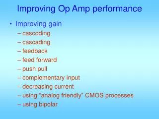
Improving Op Amp performance. Improving gain cascoding cascading feedback feed forward push pull complementary input decreasing current using “analog friendly” CMOS processes using bipolar. Improving speed Increasing UGF, increase transient speed

E N D
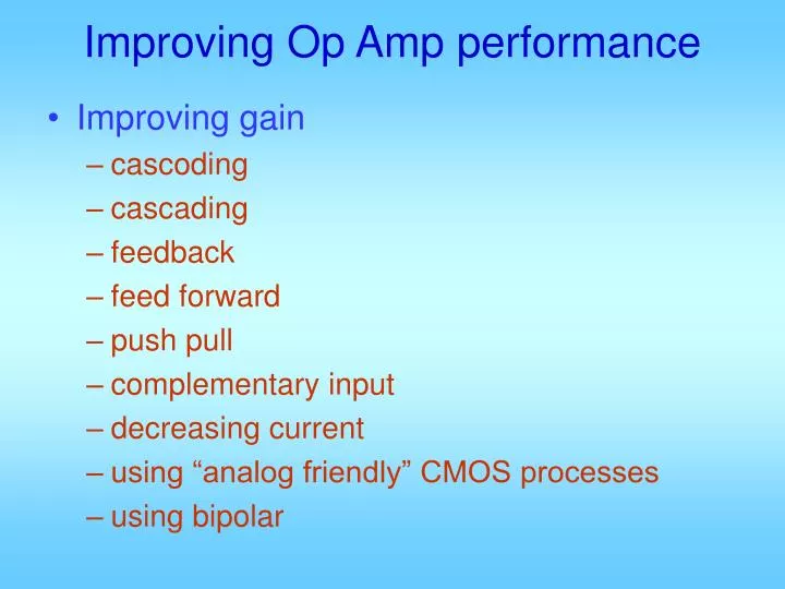
Improving Op Amp performance • Improving gain • cascoding • cascading • feedback • feed forward • push pull • complementary input • decreasing current • using “analog friendly” CMOS processes • using bipolar
Improving speed • Increasing UGF, increase transient speed • Settling may not improve, which depends on PM and secondary poles • Cannot simply increase W/L ratio optimal sizing for a given CL • Two stage optimal design: can potentially achieve higher UGF than single stage • Increasing PM at UGF, reduce ringing • Once PM large enough, no effect • Taking care of secondary poles and zeros, reduce settling time to 1/A0 level • Pole zero cancellation be accurate and at sufficiently high frequency • Cascode or mirror poles sufficiently high frequency • Reduce parasitic capacitances • Increasing current • Using better processes
Other specifications to improve • reduced power consumption • low voltage operation • low output impedance (to drive resistive load, or deliver sufficient real power) • large output swing (large signal to noise ratio) • large input common mode range • large CMRR • large PSRR • small offset voltage • improved linearity • low noise operation • common mode stability
Two-Stage Cascode Architecture • Why Cascode Op Amps? • Control the frequency behavior • Increase PSRR • Simplifies design • Where is the Cascode Technique Applied? • First stage - • Good noise performance • May require level translation to second stage • Requires Miller compensation • Second stage - • Increases the efficiency of the Miller compensation • Increases PSRR • Folded cascode op amp • Reduce # transistors stacked between Vdd and Vss
VDD VDD M9 M1 M3 M2 M4 M8 Vyy M7 M6 Vxx M5 Vbb CL CL Vin+ Vin- Differential Telescopic Cascoding Amplifier Needs CMFB On either Vyy Or VG9
Single-ended telescopic cascoding Analysis very similar to non-cascoded version: think of the cascode pair as a composite transistor. M2-MC2 has gm=gm2 go=gds2*gdsC2/gmC2 Ao=gm/go p1=-go/Co Right half plane zero: gm/Cgd2
Output swing is much less Vo1 max: VDD – Vsg3-I1*R + |VTP| Vo1 min: Vicm – Vgs1 – Vbias – VTN > Vss + Vdssat5 – Vbias – VTN Several additional pole-zero pairs At node D2-SC2: Pole: g=gmC2+gmbC2+gds2+gdsC2 C=CgsC2+cgd2+cdb2 p=-g/C ≈-gmC2/(CgsC2+cgd2+cdb2) Zero: z≈-gmC2/CgsC2 Pole-zero cancellation at -2pfT of MC2
Two stage M4 M4 bias3 M3 M3 bias2 bias1 M2 M2 Vi1 M1 M1 Vi2 CMFB Mb Depends on supply and first stage biasing, may need level shifting Analysis very similar, except very small go1, more p/z
Cascoding the second stage Very similar analysis, very small go Not suitable for low voltage design
A balanced version Mirror gain M: gm6:gm4 = gm8:gm3 * gm11:gm10 SR=I6/CL GB=gm1M/CL Ao = gm1/go * M Should have small current in these But parasitic poles should be high enough
Layout of cascode transistors With double poly: In a single poly process:
Folded cascode Balanced has better output swing and better gain than telescopic cascode Both single stage Neither require compensation But balanced limits input common mode range due to diode connection folding
VDD VDD CL folded cascode amp Same GBW as telescopic 3 4 Iss determines slew rate Vbb 6 5 Vin+ Vin- 1 2 10 11 Iss 9 8 Differential amp requires CMFB
I1=I2=Iss/2, I3=I4=Iss*1.2~1.5 • Ao=gm1/go; go=gds9*gds11/gm11 + (gds1+gds3)*gds5/gm5; • p1=-go/CL; GB = gm1/CL • Slew rate: Iss/CL • Vomin = Vg11–VTN, Vomax=Vg5+|VTP| • Vicmmin = vs+Vgs1, vicmmax=Vg3+VTN+|VTP| • Power = (Vdd-Vss)*(I3+I4) + biasing power
Appropriate Rz moves zero to cancel p2 VDD VDD VDD CL Triode transistor Vb Vb 3 4 15 Vx 5 Cc vo+ vo1- Vin+ Vin- 1 2 Rz 11 Vy Iss 13 9 Vb CMFB The left side cascode and second stage not shown
VDD VDD VDD CL NMOS11b serves as Rz Vb 3 4 Vb 15 Triode transistor vx 5 Cc vo+ vo1- Vin+ Vin- 1 2 11a Iss 13 Vy 11b Vb 9 CMFB
VDD VDD 4 Vb 15 Vbx 5 Cc CL vo+ vo1- Vin- 2 11a Iss 13 Vby 11b Vb 9 CMFB
High speed low voltage design • Assume VDD-VSS<VTN-VTP, assume a given Itot • Use minimum length for high speed operation • Use appropriate Von13,15 to achieve balance between high fT and high swing • Select Von4,5,9,11 so that vo1 has + – 10% (VDD-VSS) swing • Set desired vocm at (VDD+VSS+Vdssat13-Vsdsat15)/2 • Size transistors so that Vgs13 = mid range of vo1 swing
Show that the compensation scheme has very similar pole splitting effect as in 7 transistor op amp before • Show that appropriate sizing of M11b can cause the zero to move over p2 • If CMFB is applied at G3,4, compensation can be connected to channel of M9 • Show that with an appropriate attenuator, the go at vo1 can be made zero by positive feedback from opposite side vo1+ to G5 • Show that with an appropriate gm5, the go at vo1 can be made zero by positive feedback from opposite side vD12 to G5
PUSH-PULL Output Stage v v At low frequency, vg7 and vg8 nearly constant as vo swings
PUSH-PULL Output Stage • Let AI be the current gain from M1 to M7 • Icc=sCcVg6, (Iss-Icc)/2–>I3, DI7=AI*Icc/2 • KCL at D6: -Icc + Vg6*gm6 +DI7=0, Can choose AI so that z cancels p2 for high speed
VDD VDD VDD CL True push pull 3 4 5 Vin+ Vin- 1 2 Iss 6 Problem: bias current in second stage unknown
VDD VDD VDD CL If VDD-VSS is sufficient 3 4 5 Vbn Vbp Vin+ Vin- 1 2 6 But gain of 1st stage reduced! Iss
VDD VDD VDD VDD To recover gain: CL 3 4 5 Vbp Vbn Vin+ Vin- 1 2 6 Iss
VDD VDD VDD VDD 3 4 5 Vbp Vbn CL Vin+ Vin- 1 2 6 Iss
Figure 7.11 in book: process variations can cause large change in M21/22 current, and mismatch in M21 vs M22 bias results in offset voltage
Figure 7.1-2 Same comment applies to this one Both can have very small quiescent current when vin≈0 But provide large charging or discharging current power efficiency
Dynamically Biased (Switched) Amplifiers • Switched amplifiers lead to smaller parasitic capacitors and therefore higher frequency response. • Switched amplifiers require a non-overlapping clock • Switched amplifiers only work during a portion of a clock period • Bias conditions are setup on one clock phase and then maintained by capacitance on the active phase • Switched amplifiers use switches and capacitors resulting in feed-through problems • Simplified circuits on the active phase minimize the parasitics
Dynamically Biased Amplifiers • Two phase non-overlapping clocks
Dynamically Biased Inverter In f2 offset and bias are sampled In f1, COS provides offset cancellation plus bias for M1; CB provides the bias for M2.
VDD - VB2 - vIN vIN - VSS - VB1
A Dynamic Op Amp which Operates on Both Clock Phases True push-pull Single stage Differential-in Single-ended out No tail current Off-set cancelled For large swing: Remove cascodes S. Masuda, et. al., 1984
LOW VOLTAGE OP AMPS • We will cover: • Low voltage input stages • Low voltage bias circuits • Low voltage op amps • Examples • Methodology: • Modify standard circuit blocks for reduced power supply voltage • Explore new circuits suitable for low voltage design
Low-Voltage, Strong-Inversion Operation • Reduced power supply means decreased dynamic range • Nonlinearity will increase because the transistor is working close to VDS(sat) • Large values of λ because the transistor is working close to VDS(sat) • Increased drain-bulk and source-bulk capacitances because they are less reverse biased. • Large values of currents and W/L ratios to get high transconductance • Small values of currents and large values of W/L will give smallVDS(sat) • Severely reduced input common mode range • Switches will require charge pumps
Input common mode range drop VDD – VDS3sat + VT1 > vicm > VDS5sat + VT1 + VEB1 1.25 -0.25 + 0.75 > vicm > 0.25+0.75+0.25
p-n complementary input pairs n-channel: vicm > VDSN5sat + VTN1 + VEBN1 p-channel: vicm <VDD- VDSP5sat - VTP1 - VEBP1
Rail-to-rail constant gm input Coban and Allen, 1995
Bulk-Driven, n-channel Differential Amplifier I1=I2=I5/2 As Vic varies, Vd5 changes and gmb varies Varied gain, slew rate, gain bandwidth; nonlinearity; and difficulty in compensation
Bulk-driven current mirrors Increased vin range and vout range