Download
1 / 28
280 likes | 403 Vues
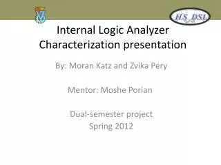
Internal Logic Analyzer F inal presentation-part A. By: Moran Katz and Zvika Pery Mentor: Moshe Porian Dual-semester project Spring 2012. Agenda . Overview Goals Requirements Architecture Data transfer Internal Logic Analyzer Core Registers Write controller Read controller RAM

E N D
Internal Logic AnalyzerFinal presentation-part A By: Moran Katz and Zvika Pery Mentor: Moshe Porian Dual-semester project Spring 2012
Agenda • Overview • Goals • Requirements • Architecture • Data transfer • Internal Logic Analyzer Core • Registers • Write controller • Read controller • RAM • In out coordinator • Simulations • Problems & solutions • Part B work plan • Schedule
Project Overview Logic Analyzer- Debugging tool for FPGA Contains software & hardware Common Logic Analyzer tools today: Hardware: Change FPGA code Memories to store data Logic to change configuration Software: Include GUI Choose trigger, data location, signals name, record results Altera- Signal Tap Xilinx- Chip Scope
Project goals • Design an internal logic analyzer to the FPGA which will be an independent part • Hardware: (1) VHDL (2) Record the chosen signals (3) Send it back to the user • Software: (1) GUI- allow to present the recorded information (2) Send request to change hardware according user’s choise (3) Build a system to check our implementation Signal Generator UART IN RX PATH TX PATH WBS WBM WBM GUI Internal Logic Analyzer Core 50 MHZ 100 MHZ WhishBone intercon Clock & Reset XILINX- SPARTAN 3E ALTERA- CYCLON II Reset Reset WBS WBS UART OUT WBM WBM- Whishbone Master WBS-Whishbone Slave FPGA Altera Cyclone II
Requirements • Option to choose the parameters • Save the recorded information and present it using waveform • Internal communication is through Wishbone protocol • External communication is through UART protocol Save and load settings Duration of recording position of trigger Type of trigger, for example ‘rise’ Signals name, which signals to record 30%-70% 50%-50% 70%-30%
Top Architecture Signal Generator UART IN TX PATH RX PATH WBS WBM WBM GUI Internal Logic Analyzer Core 50 MHZ 100 MHZ WhishBone intercon Clock & Reset Reset Reset WBS WBS UART OUT WBM WBM- Whishbone Master WBS-Whishbone Slave FPGA Altera Cyclone II
Data Transfer injecting signals behavior Trigger- first signal Recording time- 50% Signal’s number-2 signal Signal Generator UART IN signal RX PATH TX PATH WBS signal WBM WBM GUI Internal Logic Analyzer Core 50 MHZ 100 MHZ WhishBone intercon Clock & Reset Reset Reset WBS Recorded data WBS UART OUT WBM WBM- Whishbone Master WBS-Whishbone Slave FPGA Altera Cyclone II
The Core • The core is build from 7 entities: • WBS • Registers • Write Controller • RAM • Read Controller • Data Coordinator • WBM • The core tasks: • Getting and saving user configurations • Getting new data each clock cycle and saving it • Getting new trigger signal each clock cycle and check for trigger rise according user configurations • Outputting relevant data back to user
The Core Generic table 1 0 - Reset active Low, 1- Reset active High reset_polarity_g 2 enable_polarity_g 0 - Enable active Low, 1- Enable active High 3 signal_ram_depth_g depth of basic RAM signal_ram_width_g 4 width of basic RAM 5 record_depth_g number of bits that is recorded from each signal data_width_g 6 defines the width of the data lines of the system 7 Add_width_g width of address word in the RAM (Gets record_depth_g) 8 num_of_signals_g number of signals that will be recorded simultaneously 9 power2_out_g RAM output width is multiplied by this power factor '-1' => RAM output width > input width '1' => RAM input width > output width 10 power_sign_g 11 type_d_g Type Depth. type is the WB client which the data is directed to 12 len_d_g Length of the WB data (in words)
Registers • Saves the user configurations • Sends out the configurations to the WC configuration TYPE POSITION
Registers • The inputs are Register’s address and data in • Valid signal rises and data in signal is being sampled to the relevant register according to the address • From now on, the data is available at the output ADDRESS DATA IN
Write Controller • Gets the data from the signal generator and saves it in the RAM • Gets the trigger signal and looks for trigger rise according configurations DATA IN DATA IN VALID START ADDRESS TRIGGER ADDRESS TYPE POSITION
Write Controller • Trigger and data are entering each cycle • Data address and validity are being calculated and are being sent to the RAM • Trigger is compared to the configuration to identify trigger rise • If necessary start address is calculated according to the position and is being sent out ? TRIGGER POSITION TYPE START ADDRESS AOUT VALID ADDRESS DATA IN
Read Controller • Gets the start address from the WC • Extracting the relevant data from the RAM • Sends the data out to the in_out_coordinator ADDRESS DATA OUT DATA VALID START ADDRESS
Read Controller • Start address is received • The next address is calculated and sent to the RAM • Data and validity is received from RAM • Output data is being sent to the coordinator START ADDRESS ADDRESS TO RAM DATA VALID DATA FROM RAM DATA TO COORDINATOR
In Out Coordinator • Gets data and valid in from Read Controller • Sends out the data and valid out to WBM DATA VALID DATA DATA OUT VALID DATA OUT
In Out Coordinator • Data in is being sampled when valid is high • Data out is being sent out according to width_out_generic DATA IN VALID DATA OUT VALID DATA OUT DATA IN
Simulations • At first we made a manual simulation to each entity to check the functionality • Afterwards, we built a core test bunch in order to check the entire core Internal Logic Analyzer Core WBS WBM
Simulations • Each diagram was checked and confirmed for the correct result and if necessary, code changes was made and the simulation was made again. ?
Simulations • Data is insert to the registers, in order to configure the user trigger position and type • Enable signal is written to the register to enable the system • Number of signals is 5, meaning our input data is between 0-32 in decimal (2^5), at first the trigger position is 100 and all the data is recorded before the trigger, and second time the position is 0 and all the data is recorded after the trigger. For example: (test number 3)
Simulations • After that all the relevant data has being sent out, read controller finish working • We can now configure a new and different simulation • Write controller is finish • Read controller starting to send the relevant data out • Data is being save in the RAM until trigger rise • Since position is 100, we do not save data after trigger rise
Simulations • Read controller is extractiong all the 8 samples, starting from 24 (trigger rise) • When finish, read controller finish signal is rise, and the system is ready for another configuration • Since position is 0, all the data is recorded after trigger rise • After WC finish saving all the data, the RC is starting to extract the data and send it out
Problems & Solutions • After first trigger rise, the system identify another trigger rise although the data was still recorded • Problem- there was no dependency between two trigger rises • Our solution- adding wc_finish signal to the registers and resetting the enable register First example: (problem that occurred in the middle presentation)
Problems & Solutions • Input width is num_of_signals_g, output width is data_width_g • Problem- the two widths don’t match • Our solution- adding an entity who coordinate between them Second example: output width (bus) did not match the input width DATA OUT VALID DATA OUT IN OUT COOARDINATOR DATA OUT VALID DATA OUT
Working Systems • File sharing- via SVN • Coding Guidelines- code design according known conventions, usage of entity template • Code Review- 1. Visual/ Compiler 2. Local simulation to the entity 3. Top simulation
Part B- work plan • Creating Signal Generator • Integration with external blocks (rx/tx path, WB interconand others) • Simulations to the whole system • Synthesis • Building and connecting the GUI • Connecting to FPGA in the lab
Schedule 0.5 חן