Download
1 / 11
230 likes | 795 Vues
Chapter 3-2. Diffusion and band bending. We will learn two new topics in this lecture:. Diffusion – a process whereby particles tend to spread out or redistribute as a result of their random thermal motion, migrating on a macroscopic scale from regions of high particle concentration

E N D
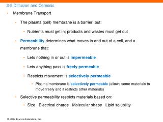
Chapter 3-2. Diffusion and band bending We will learn two new topics in this lecture: Diffusion – a process whereby particles tend to spread out or redistribute as a result of their random thermal motion, migrating on a macroscopic scale from regions of high particle concentration to region of low particle concentration. • Examples of diffusion: • Perfume in a room • Ink drop in a bottle of water • Hot point probe measurements Band bending – resulting from the presence of electric field inside a semiconductor. No band bending means the electric field is zero.
Hot-point probe measurement This is a commonly used technique for determining whether a semiconductor is p-type or n-type. Carriers diffuse more rapidly near the hot probe. This leads to a particle current away from the hot probe and an electrical current away (p-type) or towards (n-type) the hot probe.
Diffusion current • For diffusion to occur, there must be a concentration gradient. • Logically, greater the concentration gradient, greater the flux • of particles diffusing from higher concentration region to lower • concentration region. If F is the flux (i.e. the # of particles / (cm2 s) crossing a plane perpendicular to the particle flow, then, = particle concentration where D is called the diffusion coefficient. The () sign appears because for positive concentration gradient, d/dx, the particles diffuse along the negativex direction.
Particle diffusion Concentration gradient, d/dx = positive Concentration, x Particles flow along x direction
Electrons Holes x x hole flux hole diffusion current Jp | diff = qDp (dp/dx) Diffusion current electron flux electron diffusion current Jn | diff = + qDn (dn/dx) What is the unit of diffusion coefficient, D?
Total currents diffusion drift The total current flowing in semiconductor is given by: J = Jn + Jp
E EC Ei EV EC Ei EV x x No E-field indicates presence of E-field Band bending • Band diagram represents energies of electrons – so far we have drawn it as independent of position. • When E-field is present, EC and EV change with position - called “band-bending”. • This is a way to represent that an E-field is present. E
Band bending and electrostatic variables Diagram represents total energy of electrons with x K.E. = EEC for electrons P.E. = EC Eref for electrons From elementary physics P.E. = q V for electrons V = (1/q) (EC Eref) E= (dV / dx) = (1/q) (dEC/dx)
Band bending • Crudely, inverting EC (in eV) versus x diagram results in electrostatic potential V (in Volts) versus x diagram. Similar to potential energy, V is relative with respect to some arbitrary reference. • If EC Eref is given in eV, we use e = 1.6 1019 C toconvert from eV to Joules. Thus, values of V in Volts are numerically equal to EC Eref expressed in eV. • The slope of EC (energy in eV) versus x diagram gives the E-field versus x plot. E-field expressed in V/cm will be numerically equal to dEi /dx if Ei is in eV and x in cm
Example 1: (Exercise 3.2) Plot electrostatic potential, V, andE-field, E, versus x for the case shown below.
Review Resistivity formula Drift current density Diffusion current density Total hole and electron current density J = Jn + Jp Total current density