Download
1 / 33
340 likes | 659 Vues
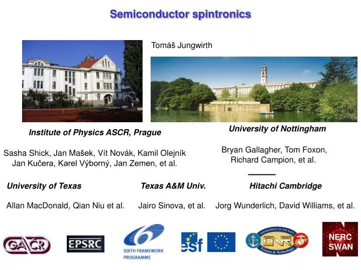
NERC SWAN. Semiconductor spintronics. Tom áš Jungwirth. Universit y of Nottingham Bryan Gallagher, Tom Foxon, Richard Campion, et al. Institute of Physics ASCR, Prague Sasha Shick , Jan Ma šek, Vít Novák, Kamil Olejník Jan Kučera, Karel Výborný, Jan Zemen, et al.

E N D
NERC SWAN Semiconductor spintronics Tomáš Jungwirth University of Nottingham Bryan Gallagher, Tom Foxon, Richard Campion, et al. Institute of Physics ASCR, Prague Sasha Shick, Jan Mašek,Vít Novák, Kamil Olejník Jan Kučera, Karel Výborný, Jan Zemen, et al. University of Texas Texas A&MUniv. Allan MacDonald, Qian Niu et al. Jairo Sinova, et al. Hitachi Cambridge Jorg Wunderlich, David Williams, et al.
1.Basic physical principles of the operation of spintronic devices 2.Current metal spintronics in HDD read-heads and memory chips 3. Research in semiconductor spintronics 4. Summary
Electron has a charge (electronics) and spin (spintronics) Electrons do not actually “spin”, they produce a magnetic moment that is equivalent to an electron spinning clockwise or anti-clockwise
quantum mechanics & special relativity particles/antiparticles & spin Dirac equation E=p2/2m E ih d/dt p -ih d/dr . . . E2/c2=p2+m2c2 (E=mc2 for p=0) high-energy physics solid-state physics and microelectronics
e- Resistor classical spintronic external manipulation of charge & spin internal communication between charge & spin
total wf antisymmetric = * spin wf symmetric (aligned) orbital wf antisymmetric e- FERO MAG NET many-body Pauli exclusion principle & Coulomb repulsionFerromagnetism • Robust(can be as strong as bonding in solids) • Strong coupling to magnetic field • (weak fields = anisotropy fields needed • only to reorient macroscopic moment)
p s V e- Beff relativistic single-particle Spin-orbit coupling (Dirac eq. in external field V(r) & 2nd-order in v /c around non-relativistic limit) • Current sensitive to magnetization • direction
1.Basic physical principles of the operation of spintronic devices 2.Current metal spintronics in HDD read-heads and memory chips 3. Research in semiconductor spintronics 4. Summary
Current spintronics applications First hard disc(1956) - classical electromagnet for read-out 1 bit: 1mm x 1mm MB’s From PC hard drives ('90) to micro-discs - spintronic read-heads 1 bit: 10-3mm x 10-3mm 10’s-100’s GB’s
Anisotropic magnetoresistance (AMR) read head 1992 - dawn of spintronics Appreciable sensitivity, simple design, scalable, cheap Giant magnetoresistance (GMR) read head - 1997 High sensitivity and are almost on and off states: “1” and “0” & magnetic memory bit
MEMORY CHIPS .DRAM(capacitor) - high density, cheep x high power, volatile .SRAM(transistors) - low power, fast x low density, expensive, volatile .Flash (floating gate) - non-volatilex slow, limited lifetime, expensive Operation through electron chargemanipulation
MRAM – universal memory fast, small, low-power, durable, and non-volatile 2006- First commercial 4Mb MRAM
Based on Tunneling Magneto-Resistance (similar to GMR but insulating spacer) RAM chip that actually won't forget instant on-and-off computers
Based on Tunneling Magneto-Resistance (similar to GMR but insulating spacer) RAM chip that actually won't forget instant on-and-off computers
1.Basic physical principles of the operation of spintronic devices 2.Current metal spintronics in HDD read-heads and memory chips 3. Research in semiconductor spintronics 4. Summary
One Ga Mn As Mn Dilute moment nature of ferromagnetic semiconductors • Key problems with increasing MRAM capacity (bit density): • Unintentional dipolar cross-links • External field addressing neighboring bits 10-100x weaker dipolar fields Current induced switching replacing external field Tsoi et al. PRL 98, Mayers Sci 99 10-100x smaller Ms 10-100x smaller currents for switching Sinova et al., PRB 04, Yamanouchi et al. Nature 04
Ga Mn As Mn Ferromagnetic semiconductors More tricky than just hammering an iron nail in a silicon wafer GaAs - standard III-V semiconductor Group-II Mn - dilute magnetic moments & holes (Ga,Mn)As - ferromagnetic semiconductor
Ga Mn >2% Mn As Mn GaAs:Mn – extrinsic p-type semiconductor EF spin << 1% Mn ~1% Mn DOS Energy spin onset of ferromagnetism near MIT As-p-like holes localized on Mn acceptors valence band As-p-like holes As-p-like holes with 5 d-electron local moment on the Mn impurity Mn-d-like local moments Jungwirth et al. RMP ‘06
~100 nm Dipolar-field-free current induced switching nanostructures see J. Zemen 12:05, T2 Micromagnetics (magnetic anisotropy) without dipolar fields (shape anisotropy) One Domain wall Can be moved by ~100x smaller currents than in metals Humpfner et al. 06, Wunderlich et al. 06 Strain controlled magnetocrystalline (SO-induced) anisotropy
Q VD Source Drain Gate VG M [010] [110] F [100] [110] [010] Coulomb blockade AMR spintronic transistor Anisotropic chemical potential magnetic electric & control of CB oscillations Wunderlich et al. PRL 06
CBAMR SET • Combines electrical transistor action • with magnetic storage • Switching between p-type and n-type • transistor by M programmable logic
Spintronics in non-magnetic semiconductors way around the problem of low Curie T in ferromagnetic semiconductors & back to exploring spintronics fundamentals
V Spintronics relies on extraordinary magnetoresistance Ordinary magnetoresistance: response in normal metals to external magnetic field via classical Lorentz force Extraordinary magnetoresistance: response to internal spin polarization in ferromagnets often via quantum-relativistic spin-orbit coupling B anisotropic magnetoresistance _ _ _ _ _ _ _ _ _ _ _ FL + + + + + + + + + + + + + I V _ _ FSO M _ I e.g. ordinary (quantum) Hall effect and anomalous Hall effect Known for more than 100 years
majority _ _ _ FSO _ FSO I minority _ _ _ FSO _ non-magnetic FSO I p s V Beff V V=0 Spin-orbit coupling skew scattering intrinsic Anomalous Hall effect in ferromagnetic conductors: spin-dependent deflection & more spin-ups transverse voltage Spin Hall effect in non-magnetic conductors: spin-dependent deflection transverse edge spin polarization
n p n Cu Spin Hall effect detected optically in GaAs-based structures Same magnetization achieved by external field generated by a superconducting magnet with 106 x larger dimensions & 106 x larger currents SHE microchip, 100A superconducting magnet, 100 A Wunderlich et al. PRL 05 SHE edge spin accumulation can be extracted and moved further into the circuit SHE detected elecrically in metals
1.Basic physical principles of the operation of spintronic devices 2.Current metal spintronics in HDD read-heads and memory chips 3. Research in semiconductor spintronics 4. Summary
Ferro Ga Magnetization Mn As Mn Current Spintronics explores new avenues for: • Information reading • Information reading & storage Tunneling magneto-resistance sensor and memory bit • Information reading & storage & writing Current induced magnetization switching • Information reading & storage & writing & processing Spintronic single-electron transistor: magnetoresistance controlled by gate voltage • Materials: Dilute moment ferromagnetic semiconductors & non-magnetic – spin Hall effect
Materials research of DMSs In (Ga,Mn)As Tc ~ #MnGa (Tc=170K for 6% MnGa) But the SC refuses to accept many group-II Mn on the group-III Ga sublattice III = I + II Ga = Li + Zn • GaAs and LiZnAs are twin SC • (Ga,Mn)As and Li(Zn,Mn)As • should be twin ferromagnetic SC • But Mn isovalent in Li(Zn,Mn)As • no Mn concentration limit • possibly both p-type and n-type ferromagnetic SC (Li / Zn stoichiometry) Masek et al. PRL 07
Ga Mn As Mn (Ga,Mn)As material 5 d-electrons with L=0 S=5/2 local moment moderately shallow acceptor (110 meV) hole -Mn local moments too dilute (near-neghbors cople AF) - Holes do not polarize in pure GaAs - Hole mediated Mn-Mn FM coupling
Ga Mn As Mn Mn–hole spin-spin interaction As-p Mn-d hybridization Hybridization like-spin level repulsion Jpd SMn shole interaction
Mn As Ga Ferromagnetic Mn-Mn coupling mediated by holes heff = Jpd <SMn> || x Hole Fermi surfaces Heff = Jpd <shole> || -x