Download
1 / 14
140 likes | 504 Vues
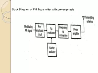
A LOW COST LONG RANGE FM TRANSMITTER WITH AUDIO MODULATION. Introduction. The FM transmitter has 3 stages, A (VFO) Variable frequency Oscillator (30 mw), a class C driver stage (150 mw) and a class C final power amplifier (1 Watt).

E N D
A LOW COST LONG RANGE FM TRANSMITTER WITH AUDIO MODULATION
Introduction The FM transmitter has 3 stages, A (VFO) Variable frequency Oscillator (30 mw), a class C driver stage (150 mw) and a class C final power amplifier (1 Watt). Basically every FM Transmitter has to have a Voltage Controlled Oscillator (VCO). This is a high frequency oscillator whose output frequency changes based on the voltage applied at a particular control point. This is a variable frequency oscillator (VFO).
EMBEDDED SYSTEMS Definition for :- EMBEDDED SYSTEMS • A combination of hardware and software which together form a component of a larger machine. • An example of an embedded system is a microprocessor that controls an automobile engine. • An embedded system is designed to run on its own without human intervention, and may be required to respond to events in real time.
Contents Introduction Block diagram Hardware requirements Power supply Schematic diagram Working of the project Advantages Applications Conclusion
555 TIMER The 555 Timer IC is an integratedcircuit (chip) implementing a variety of timer and multivibrator applications • The 555 has three operating modes: • Monostable mode: in this mode, the 555 functions as a "one-shot". Applications include timers, missing pulse detection, switches, touch switches, frequency divider, capacitance measurement, pulse-width modulation (PWM) etc. • Astable - free running mode: the 555 can operate as an oscillator. Uses include LED and lamp flashers, pulse generation, logic clocks, tone generation, security alarms, pulse position modulation, etc. • Bistable mode or Schmitt trigger: the 555 can operate as a flip-flop, if the DIS pin is not connected and no capacitor is used. Uses include bounce free latched switches, etc.
LM358 (DUAL OPERATIONAL AMPLIFIER) • The LM358 series consists of two independent, high gain; internally frequency compensated operational amplifiers which were designed specifically to operate from a single power supply over a wide range of voltages • Operation from split power supplies is also possible and the low power supply current drain is independent of the magnitude of the power supply voltage. Pin description 1 ) Output 1 2 )Inverting input 3 ) Non-inverting input 4 )VCC- 5 )Non-inverting input 2 6 ) Inverting input 2 7 ) Output 2 8 ) VCC+
LM339( COMPARATOR) • The LM339 consists of four independent precision voltage comparators • The LM339 series was designed to directly interface with TTL and CMOS. • When operated from both plus and minus power supplies, the LM339 series will directly interface with MOS logic where their low power drain is a distinct advantage over standard comparators.
FEATURES • Wide single supply voltage range 2.0VDC TO 36VDC or dural supplies ±1.0VDC to ±18VDC • ● Very low supply current drain (0.8㎃) independent • of supply voltage (1.0㎽/comparator at 5.0VDC) • ● Low input biasing current 25㎁ • ● Low input offset current ±5㎁ and offset voltage • ● Input common-mode voltage range includes ground • ● Differential input voltage range equal to the power • supply voltage • ● Low output 250㎷ at 4㎃ saturation voltage • ● Output voltage compatible with TTL, DTL, ECL, MOS and CMOS logic system • ● Moisture Sensitivity Level 3
BC547 (NPN –Transistor) • The BC547 transistor is an NPN Epitaxial Silicon Transistor. • It is used in general-purpose switching and amplification BC847/BC547 series 45 V, 100 mA NPN general-purpose transistors. • The ratio of two currents (Ic/Ib) is called the DC Current Gain of the device and is given the symbol of hfe or nowadays Beta, (β).
The current gain from the emitter to the collector terminal, Ic/Ie, is called Alpha, (α), and is a function of the transistor itself
BATTERY • An electrical battery is a combination of one or more electrochemical cells, used to convert stored chemical energy into electrical energy. • The battery has become a common power source for many household, robotics and industrial applications. • Larger batteries provide standby power for telephone exchanges or computer data centers