Download
1 / 35
350 likes | 359 Vues
DMT 234 Semiconductor Physic & Device. Lecture 2 The Crystal Structure of Solids. Mnorhafiz 2011. DMT 234 Semiconductor Physic & Device. Preview. This topic expalin about basic properties and characteristics of semicondcutor material. Mnorhafiz 2011. DMT 234 Semiconductor Physic & Device.

E N D
DMT 234 Semiconductor Physic & Device Lecture 2The Crystal Structure of Solids Mnorhafiz 2011
DMT 234 Semiconductor Physic & Device Preview • This topic expalin about basic properties and characteristics of semicondcutor material. Mnorhafiz 2011
DMT 234 Semiconductor Physic & Device Semiconductor Materials • Semiconductor are a group of materials having conductivities between of metal and insulators. • Single element - elemental semiconductor • •More than one element - compound semiconductor Mnorhafiz 2011
DMT 234 Semiconductor Physic & Device Type of Solids • Three general types – Characterized by the size of an ordered region within the material. • Amorphous – little or no order. Order with a few atomic or molecular dimensions. • Polycrystalline – High degree of order within limited regions which vary in size and orientation to each other. • Single Crystal – High degree of order throughout the entire volume of the material. Mnorhafiz 2011
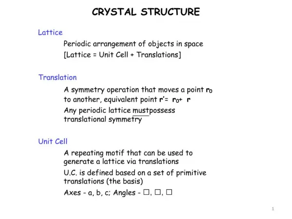
DMT 234 Semiconductor Physic & Device Space Lattices • The regular geometric periodicity in the atomic arrangement. • Lattice – the three dimensional periodic arrangement of atoms (or group of atoms) in the crystal. • Lattice point – a particular atomic array shown by a dot. These dots are separated (translated) in certain directions and dimensions • Unit Cell – a small volume of the crystal that can be used to reproduce the entire crystal. Mnorhafiz 2011
DMT 234 Semiconductor Physic & Device Primitive cell and lattice vector • Primitive cell – is the smallest unit cell that can be repeated to form the lattice. This may not be the most convenient cell to use for analysis. • Lattice vector – every equivalent lattice point in the three-dimensional crystal can be found by using the vector : • Where p, q and s are integers. Mnorhafiz 2011
DMT 234 Semiconductor Physic & Device Basic Crystal Structures • The easiest 3-D lattice to work with is the simple cubic lattice (SCC) which has lattice points on all the corners of a cube. The Cubic (Isometric) crystal system is characterized by its total symmetry. • It has three crystallographic axes that are all perpendicular to each other and equal in length. • The cubic system has one lattice point on each of the cube's four corners. Mnorhafiz 2011
DMT 234 Semiconductor Physic & Device Crystal Planes abd Miller Indices • Semiconductor devices are fabricated at or near the crystal surface. Thus the surface properties influence the device characteristics. • Surface or plane through the crystal can be described by the intercepts of the plane along the a, b and c axes used for the lattice. Mnorhafiz 2011
DMT 234 Semiconductor Physic & Device Miller Indices The plane (a) is parallel to the b and c axes so the intercepts are given as 1,infinite and infinite. Taking reciprocal, we obtain Miller indices as (1,0,0), so the plane is referred to as (100) plane. Any plane parallel to this is equivalent and is referred to as the (100) plane. • Miller Indices – describes the orientation of the plane with respect to the surface. Mnorhafiz 2011
DMT 234 Semiconductor Physic & Device Miller Indices Example The figure shows the intercepts as 3a, 2b and 1c where a,b and c the unit vectors. To form the miller indices, take the reciprocals of the intercepts. ( 1/3 , ½ , 1/1 ) Cleaar the fraction by multiplying by the lowest common denominator which is 6 in this case. ( 2,3,6) The integers are referred to as the Miller indices. The plane formed by the intercepts is the (236) plane / ( 2, 3 ,6). Mnorhafiz 2011
DMT 234 Semiconductor Physic & Device Miller Indices Example The figure shows the (100) plane. So the Miller indices are (100). How were these indices found? To form the Miller Indices, take the reciprocals of the intercepts. (1/1, 1/, 1//) = (1/1 , 0, 0) Clear the fraction by multiplying by the lowest common denominator which is 1 in this case. (100) Miller Indices state as (100). Mnorhafiz 2011
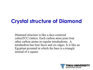
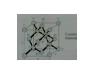
DMT 234 Semiconductor Physic & Device Diamond Structure • Silicon is the most common semiconductor material and is referred to as a group IV element. It has the diamond crystal structure. • The diamond structure is more complicated body-centered cubic. The tetrahendral structure results in each silicon atom having four nearest neighbors. • Silicon has the diamond structure. Compund semiconductors such as the binary GaAs have the zincblende structure which is the diamond structure but has two different atoms in specific places in the lattice. Mnorhafiz 2011
The tetrahedral structure is basically a body-centered cubic with four of the corner atoms missing. • Every atom in the tetrahedral structure has four nearest neighbors with equal distance. This is the basic building block of the diamond lattice.
DMT 234 Semiconductor Physic & Device Zincblend structure in GaAs Zincblend structure is similar to diamond structure, but atoms in penetrating FCC are different. Mnorhafiz 2011
DMT 234 Semiconductor Physic & Device Atomic Bonding Mnorhafiz 2011
DMT 234 Semiconductor Physic & Device Atomic Bonding • Covalent bond – Atomic bond that tends to achieve closed-valence energy shells • Ionic bond – attraction between two opposite charge ( ion and electron) and form a bond. • Metallic bond – Attraction between atomic bonding with crystal structure. • Van der waals bond – weakest chemical bond (inert gas element - He, ar etc) Mnorhafiz 2011
DMT 234 Semiconductor Physic & Device Atomic Bonding Mnorhafiz 2011
DMT 234 Semiconductor Physic & Device Atomic Bonding Mnorhafiz 2011
DMT 234 Semiconductor Physic & Device Atomic Bonding Mnorhafiz 2011
DMT 234 Semiconductor Physic & Device Imperfections in solids Lattice imperfection is any deviation from perfect periodic arrangement of lattice points. Point defects can be in the form of vacancy (missing atom), substitutional impurity (atom replaced by another atom) or interstitial impurity (additional impurity not at lattice point) Mnorhafiz 2011
DMT 234 Semiconductor Physic & Device Imperfections in solids Line Defect - Edge dislocation is a type of line defect. Mnorhafiz 2011
DMT 234 Semiconductor Physic & Device Imperfections in solids Mnorhafiz 2011
DMT 234 Semiconductor Physic & Device Imperfections in solids Mnorhafiz 2011
DMT 234 Semiconductor Physic & Device Growth of Semiconductor Materials Mnorhafiz 2011
DMT 234 Semiconductor Physic & Device Growth of Semiconductor Materials Mnorhafiz 2011
DMT 234 Semiconductor Physic & Device Growth of Semiconductor Materials Mnorhafiz 2011
DMT 234 Semiconductor Physic & Device Growth of Semiconductor Materials Mnorhafiz 2011
DMT 234 Semiconductor Physic & Device Growth of Semiconductor Materials Mnorhafiz 2011
DMT 234 Semiconductor Physic & Device Growth of Semiconductor Materials Mnorhafiz 2011
DMT 234 Semiconductor Physic & Device Growth of Semiconductor Materials Mnorhafiz 2011
DMT 234 Semiconductor Physic & Device Growth of Semiconductor Materials Mnorhafiz 2011
DMT 234 Semiconductor Physic & Device Growth of Semiconductor Materials Mnorhafiz 2011
DMT 234 Semiconductor Physic & Device Growth of Semiconductor Materials Mnorhafiz 2011
DMT 234 Semiconductor Physic & Device • Q & A • Next week Topic :The Semiconductor in Equilibrium. Mnorhafiz 2011