Download
1 / 9
190 likes | 1.26k Vues
Altera Cyclone II (484 Pin BGA). 22 Pins. 22 Pins. DE1 Pin Assignments. SW9 L2. SW7 M2. SW5 U12. SW3 V12. SW1 L21. KEY3 T21. KEY2 T22. KEY1 R21. KEY0 R22. SW8 M1. SW6 U11. SW4 W12. SW2 M22. SW0 L22. LED R9 R17. LED R7 U18. LED R5 V19. LED R3 Y19. LED R1 R19. LED G7 Y21.

E N D
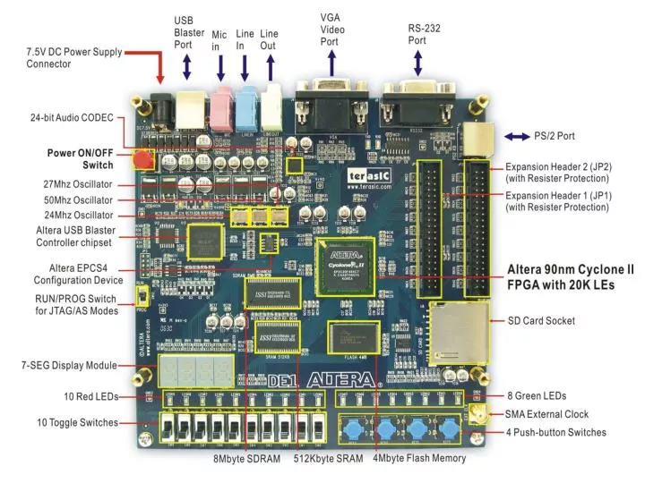
Altera Cyclone II (484 Pin BGA) 22 Pins 22 Pins
DE1 Pin Assignments SW9L2 SW7M2 SW5U12 SW3V12 SW1L21 KEY3T21 KEY2T22 KEY1R21 KEY0R22 SW8M1 SW6U11 SW4W12 SW2M22 SW0L22 LEDR9R17 LEDR7U18 LEDR5V19 LEDR3Y19 LEDR1R19 LEDG7Y21 LEDG5W21 LEDG3V21 LEDG1U21 LEDR8R18 LEDR6Y18 LEDR4T18 LEDR2U19 LEDR0R20 LEDG6Y22 LEDG4W22 LEDG2V22 LEDG0U22
0 1 5 6 4 2 3 DE1 Pin Assignments HEX3 HEX1 HEX2 HEX0 HEX0[0] PIN_J2 HEX0[1] PIN_J1 HEX0[2] PIN_H2 HEX0[3] PIN_H1 HEX0[4] PIN_F2 HEX0[5] PIN_F1 HEX0[6] PIN_E2 HEX1[0] PIN_E1 HEX1[1] PIN_H6 HEX1[2] PIN_H5 HEX1[3] PIN_H4 HEX1[4] PIN_G3 HEX1[5] PIN_D2 HEX1[6] PIN_D1 HEX2[0] PIN_G5 HEX2[1] PIN_G6 HEX2[2] PIN_C2 HEX2[3] PIN_C1 HEX2[4] PIN_E3 HEX2[5] PIN_E4 HEX2[6] PIN_D3 HEX3[0] PIN_F4 HEX3[1] PIN_D5 HEX3[2] PIN_D6 HEX3[3] PIN_J4 HEX3[4] PIN_L8 HEX3[5] PIN_F3 HEX3[6] PIN_D4
Steps in designing with Quartus II • Select target device • Design • Use VHDL, Schematics, etc. • Synthesize • Build (compile chip) • Simulate and verify • Timing simulation • Check input/output pin assignments • Change any that need to be moved • Program chip
Device Selection • Assignments | Device • Cyclone II • EP2C20F484C7
Designing/Compiling/Simulating • Use any of the following methods to make your design • Schematics (Block Diagram File – .BDF) • VHDL (.VHD) • Verilog (.V) • Leave the default settings for the compiler – just press “Play” • Use the Simulator to check your work • See tutorials (Homework 3) for a guide
Pin Assignment • Assign pins to input/output symbols • For now inputs come from switches and buttons • For now outputs go to LEDs • Use the tables from the previous slides to figure out which pins are connected to the parts you need • Select Assignments | Pins • Use the table at the bottom – ignore the rest • Enter the pin number for each I/O
Programming • First, Re-Compile after selecting Pins • Select Tools | Programmer • Power up the board (red button) • Make sure RUN/PROG is in RUN mode • Make sure USB-Blaster is specified – if not use the Hardware setup • Click Start