Download
1 / 19
190 likes | 336 Vues
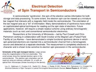
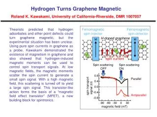
Gate Control of Spin Transport in Multilayer Graphene. By H . Goto et al. Kun Xu. Advantages. Advantages of spin over charge: Easily manipulatable with externally applied magnetic fields Long coherence/relaxation time. GMR. Giant magnetoresistance Sandwich structure FNF

E N D
Gate Control of Spin Transport in Multilayer Graphene By H. Goto et al. Kun Xu
Advantages • Advantages of spin over charge: • Easily manipulatable with externally applied magnetic fields • Long coherence/relaxation time
GMR • Giant magnetoresistance • Sandwich structure • FNF • Spin valve (HDD read/write heads) • The 2007 Nobel Prize in physics was awarded to Albert Fert and Peter Grünberg for the discovery of GMR
Disadvantages • Existing spin devices do not amplify signals
Datta-Das Device • Current modulated by the degrees of precession in electron spin introduced by the gate field
Spin-based quantum Computer • Qubit – intrinsic binary units • Quantum entanglement • Single electron trapped in a quantum dot
Spin transport in graphite based devices • Carbon nanotubes • Graphene • Multilayer graphene (MLG) • Weak spin-orbit and hyperfine interaction • Gate control of spin conduction
Device Structure • MLG Exfoliated from kish graphite • 2.5nm thick, about 7 layers (by SEM/AFM) • Doped Si/SiO2 substrate
Device Structure • 50nm Co electrodes 200nm/330nm • Separated by L=290nm
Device Structure • Cr/Au nonmagnetic electrodes • 5nm/100nm thick
Measurement • Four terminal lock-in technique • 4.2K • Excitation current of 1.0 uA, 119Hz • Back gate bias
Spin Signal: Rs • Rs=Rp-Rap • Proportional to R when FN interfaces are opaque • Proportional to 1/R when FN interfaces are transparent
Spin Signal: Rs Vn=1.5V
Spin relaxation length • MLG • Graphene: 1.5-2 um at room temperaure, may stay the same at low temperature