Download
1 / 13
130 likes | 325 Vues
R3B Heavy Ion Tracking. Roman Gernhäuser, TU-München. Status of the High Rate Diamond Detectors for Heavy Ion Tracking and TOF. detector concept larger area prototypes test experiment electronics development. R 3 B (Reactions with Relativistic Radi o active Beams) Setup.

E N D
R3B Heavy Ion Tracking Roman Gernhäuser, TU-München Status of the High Rate Diamond Detectors for Heavy Ion Tracking and TOF • detector concept • larger area prototypes • test experiment • electronics development R3B - meeting Oct 2008@ Gothenburg
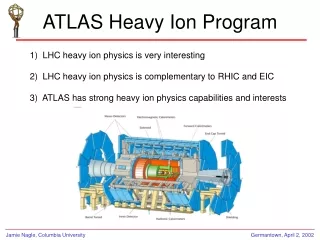
R3B (Reactions with Relativistic Radioactive Beams) Setup Dp/p ~ 10-4 @ 2.5% accept. Measurement of all kinematic variables in a HI reaction Different tasks: High resolution tracking in the super FRS, radiation hard (SFRS) 106 cm-1 s-1 2 x TOF (SFRS – target) (reaction products) low material budget R3B - meeting Oct 2008@ Gothenburg
APV APV APV APV R3B Detector Concept • tracking layer: • 50 x 50 mm, d = 100 mm, PC-CVDD • 140 mm pitch (125mm strips, 15 mm gap) • only digital position information • multiplexed readout in vacuum • timing layer: • 50 x 50 mm, d = 100 mm, PC-CVDD • 16 rate matched strips, y information, trigger • analog preamplification in vacuum • discriminator @ 5 m distance R3B - meeting Oct 2008@ Gothenburg
240 Mean charge [a.u.] 200 160 Dose [ions / mm2] ~98 % st= 75 ps expected 25 ps counts Energy [ADC ch.] 5•1010 1.5•1011 2.5•1011 Energy [ADC ch.] Time [60ps] Status 2007 • detailed investigations: • using ~ 40 x 1cm2 sample detectors • material properties checked • radiation hardness proven • segmentation scheme optimized • lithography improved (15mm) • efficiency > 98% • fast preamps vacuum suited • good TOF resolution • 1st prototype of APV readout next steps: intermediate size prototypes separate detector – electronics test of high resolution tracking R3B - meeting Oct 2008@ Gothenburg
Larger Area Detector 4 prototypes produced 2 operational lithography under control Frontside: 128 strips 170 mm wide 20 mm gap Backside: 16 strips 25.4 mm R3B - meeting Oct 2008@ Gothenburg
GTB bridge board Full system test in R3B Setup APV25 chip • 128 channels • preamplifier, shaper on board • 8 MIPS dynamic range • vacuum suitable • ADCs on GTB bridge board • 25.4 x 25.4 mm2 • 128 micro strips (200 µm ) R3B - meeting Oct 2008@ Gothenburg M.Boehmer, TU Muenchen, PhD Thesis (2006)
600 AMeV 12C 600 AMeV 124Xe multiplicity multiplicity 100 µm 100 µm trigger scintillator diamond intrinsic resolution ~ 200 μm 600 AMeV 124Xe position dia1 [0.2mm] R3B - meeting Oct 2008@ Gothenburg S. Schwertel et al., GSI Scientific Report 2007 (GSI Report 2008-1) 216
current [nA] Nr. @ 15 kHz @ 200 kHz 67 10 420 70 80 1800 74 290 1200 75 5 230 76 35 650 77 30 400 Persistent Particle Induced Currents many samples were investigated 70 % show particle induced current variation with time and producer same production parametersbut different behaviour about 50 % yield investigation of properties not yet finished 3 inch waver as grown polished beam off schematically current t [s] 1 R3B - meeting Oct 2008@ Gothenburg
Improved Samples • two step growth and • polishing process to reduce stress • round shaped corners • metallization by sputtering • Additional heat treatment • (We saw much better performance • on single crystal material) _ cut Less stress larger grains + _ + + Si substrate + R3B - meeting Oct 2008@ Gothenburg
TOF measurement small detector large detector C = 5pF 50W impedance on both sides C = 50pF APV impedance matching? R3B - meeting Oct 2008@ Gothenburg
1ns Shaping larger impedance less noise sensitive better adopted to APV simple signal transport use of standard discriminators R3B - meeting Oct 2008@ Gothenburg
Improved Electronics Impedance matching and Shaping Amplifier Discriminator TOT measurement Capacitive charge splitter APV VME R3B - meeting Oct 2008@ Gothenburg
Task List • Detector Production • New material with less persistent photo current (PPC) after irradiation • New metallization and heat treatment. • Full size detectors • Signal Properties • New shaping preamplifiers • Signal splitting to fit APV range • New discriminators • Test experiments • 48MeV Li beam in Munich (two detectors) (Nov 2008) • 1GeV beam GSI (four detectors in a row) (2009?) R3B - meeting Oct 2008@ Gothenburg