Download
1 / 20
200 likes | 336 Vues
An Implementation of the Discrete Fourier Transform on a Reconfigurable Processor. By Michael J. White 1,2 * and Clay Gloster, Jr., Ph.D., P.E. 1 1 Department of Electrical & Computer Engineering Howard University 2300 Sixth Street, NW Washington, DC 20059 2 NASA/ Goddard Space Flight Center

E N D
An Implementation of the Discrete Fourier Transform on a Reconfigurable Processor By Michael J. White1,2* and Clay Gloster, Jr., Ph.D., P.E.1 1Department of Electrical & Computer Engineering Howard University 2300 Sixth Street, NW Washington, DC 20059 2NASA/ Goddard Space Flight Center Code 564 Greenbelt, MD 20771 Michael.J.White@nasa.gov, cgloster@howard.edu *Member, AIAA MAPLD Conference Washington, DC September 9-11, 2003 P74
Outline of the Presentation • Introduction • The Discrete Fourier Transform (DFT) • A Sample Reconfigurable Processor • A Floating Point DFT Core • Experimental Results • Conclusions and Future Work P74
Introduction • A reconfigurable computing (RC) system is a hardware/software data processing system that combines the flexibility of a general purpose processors with the speed of application specific processors. • Several applications have been mapped onto RC systems demonstrating an order of magnitude speedup over existing solutions running on a general purpose processor. • In the past, RC systems contained very limited hardware resources. As a result, few complex applications, i.e. floating point arithmetic, could benefit from the potential speedup offered by RC systems. • To the knowledge of the authors, few have published papers on implementing the DFT on a Field Programmable Gate Array(FPGA) using floating point arithmetic. P74
Motivation • At Goddard, there is an interest in control algorithms, that in part use the DFT. • These algorithm should not be constrained to require the input data to be of size 2^n. • The goal is to be able to process a 512x512 floating point array in 0.01 seconds. P74
Problem Statement • Given: A software implementation of the DFT • Find: An RC system implementation of the DFT that uses floating point arithmetic such that it : • fits on a single FPGA • can handle on the order of 1000 points • execute the DFT significantly faster than the software implementation • can compute a 2D DFT more efficiently, i.e. compute the 2D DFT of a 512x512 array in 0.01 seconds P74
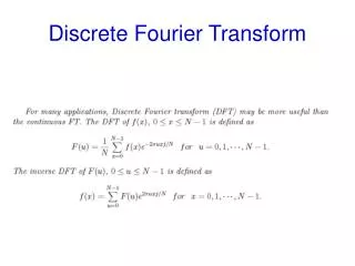
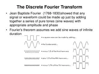
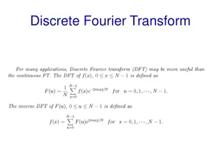
The Discrete Fourier Transform (DFT) The Discrete Fourier Transform(DFT) is defined as: X(k) = Σ c(n)*exp(-j*2*π*n*k/N) where: • c is the complex input sample • N is the total number of input samples • c(n) is the nth input sample • X(k) is the kth output sample P74
To Output Memory To Input Memory A Sample Reconfigurable Processor PECORE(FPGA) Control Unit Data Unit DFT Function Core P74
Function Core • Has one or more 32-bit inputs • Has Simple Control • Perform floating point vector operations. • - Can be built using other FunCores. P74
DATA and CONTROL UNIT • CONTROL UNIT • Manages memory read/write transactions. • Initiates instruction fetch/decode/execution • Determines when instruction processing is complete and turns control back over to the Host/Memory Interface. • One controller handles processing for all hardware modules/instructions • DATA UNIT • Contains a register file (8 32-bit registers) and counters for determining when vector instructions are complete. • Contains several memory address registers/counters for indexing through input/output vectors. • Contains up to 7 Function Cores P74
DFT Floating Point Core INPUTS OUTPUTS 32 DFT XREALIN XIMAGIN K DFT/IDFT ENABLE EMPTY 32 32 XREALOUT XIMAGOUT READYTOEMPTY DONE 10 32 32 • Xrealin/Ximagin are real and imaginary inputs • K output index • DFT/IDFT flag is –1 for DFT or 1 for Inverse DFT • Enable tells the FPGA to begin processing • Empty tells the FPGA the input buffer is empty • Xrealout/Ximagout are real and imaginary outputs. • Readytoempty says FPGA processing completed • Done tells the pipeline has been “flushed” and all outputs are in the buffer. P74
The DFT Core Block Diagram XREALIN XIMAGIN N K ENABLE 10 10 THETA UNIT * * ADDRESS 10 SIN/COS TABLE Xr 32 Xi 32 SINθ 32 COSθ 32 SELECT DFT COMPLEX MULTIPLY Yr 32 Yi 32 EMPTY COMPLEX ACCUMLATOR DONE REALOUT IMAGOUT 32 32 P74
Complex Multiply Xi COS θ Xr COS θ Xi SIN θ Xr SIN θ * * * * Select DFT Select DFT Delay Delay * * XrCOSθ XiSINθ XiCOSθ XrSINθ * * SIGOUT0 SIGOUT1 P74
Theta and Sin/Cos Units In executing the DFT, K(output index is given), that is to say we know what frequency component we to examine. A counter is used to generate n Counter K n 10 10 THETA UNIT ADDRESS 10 SIN/COS TABLE SINθ 32 COSθ 32 P74
Complex Accumulator Yr 32 Yi 32 IMAGINARY ACCUMULATOR REAL ACCUMULATOR COMPLEX ACCUMULATOR 32 32 REALOUT IMAGOUT P74
Experimental Setup • VHDL Modeling and Simulation • Logic Synthesis • Place and Route • Execute on FPGA P74
FPGA Runtime Environment RC System General Purpose Processor FPGA Board Interpreter Session File Definition File P74
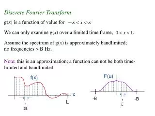
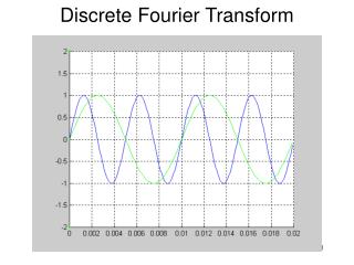
Output of DFT FPGA and Simulation The graph shows the outputs of a 10 pt floating point DFT ran on the FPGA and the output of a 10 pt DFT ran on a commercially simulation tool. P74
Conclusion • VHDL modeling and synthesis are completed. • Place and Route tool give a max clock frequency of 13.4 MHz. and 53% of FPGA is utilizes P74
Future Work • The results of FPGA implementation demonstrated an excellent correction with standard simulation tool. • Next step is to perform more checks wit DFT with larger size sample blocks and find execution speed • Start work on Floating Point Fast Fourier Transform P74
Acknowledgement • The authors would like to thank NASA/ Goddard Space Flight Center for its support of this project. In particular, we give thanks to: • Mr. Thomas Flatley and Mr. Semion Kizhner for initiating the project. • Mr. Robert Kasa and Mr. Wesley Powell for their management support. • Dr. John Day for providing the spark that put everything together. P74