Download
1 / 20
460 likes | 1.17k Vues
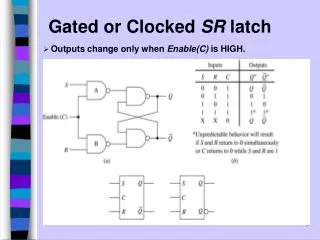
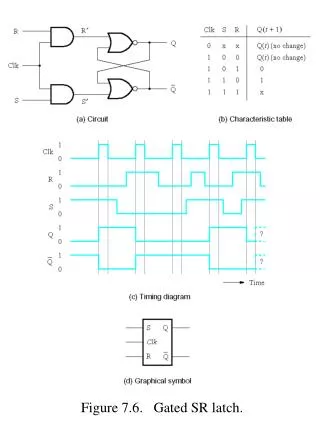
(. ). Q. t. +. 1. Clk. S. R. ¢. R. R. Q. 0. x. x. Q(. t. ) (no change). 1. 0. 0. Q(. t. ) (no change). Clk. 1. 0. 1. 0. 1. 1. 0. 1. Q. 1. 1. 1. x. S. ¢. S. (a) Circuit. (b) Truth table. 1. Clk. 0. 1. R. 0. 1. S. 0. 1. ?. Q. 0. 1. ?. Q. 0.

E N D
( ) Q t + 1 Clk S R ¢ R R Q 0 x x Q( t ) (no change) 1 0 0 Q( t ) (no change) Clk 1 0 1 0 1 1 0 1 Q 1 1 1 x S ¢ S (a) Circuit (b) Truth table 1 Clk 0 1 R 0 1 S 0 1 ? Q 0 1 ? Q 0 Time (c) Timing diagram Q S Clk R Q (d) Graphical symbol Figure 7.6. Gated SR latch.
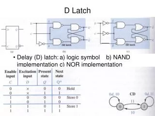
S D (Data) Q Clk Q R (a) Circuit ( ) Clk D Q t + 1 Q D ( ) Q t 0 x 1 0 0 Clk Q 1 1 1 (b) Truth table (c) Graphical symbol t t t t 1 2 3 4 Clk D Q Time (d) Timing diagram Figure 7.8. Gated D latch.
Master Slave Q Q m s Q Q D D Q D Clk Clk Clock Q Q Q (a) Circuit Clock D Q m Q = Q s (b) Timing diagram Q D Q (c) Graphical symbol Figure 7.10. Master-slave D flip-flop.
Q D D Q a Clock Q Q Clk a Q D Q b Q Q b Q D Q c Q Q c (a) Circuit Clock D Q a Q b Q c (b) Timing diagram Figure 7.12. Comparison of level-sensitive and edge-triggered.
Preset Q Clock Q D Clear (a) Circuit Preset Q D Q Clear (b) Graphical symbol Figure 7.14. Positive-edge-triggered D flip-flop with Clear and Preset.
Q D Q T Q Q Clock (a) Circuit ( ) Q t + 1 T Q T ( ) 0 Q t ( ) 1 Q t Q (b) Truth table (c) Graphical symbol Clock T Q (d) Timing diagram Figure 7.16. T flip-flop.
Q Q D 0 Enable Q Q Q D 1 Q Q Q D 2 Q Q Q D 3 Q Output carry Clock Figure 7.24. A four-bit counter with D flip-flops.
0 Enable Q Q D 0 1 D 0 Q 0 Q Q D 1 D 1 1 Q 0 Q Q D 2 D 1 2 Q 0 Q Q D 3 D 1 3 Q Output carry Load Clock Figure 7.25. A counter with parallel-load capability.
module swap (Data, Resetn, w, Clock, Extern, RinExt, BusWires); input [7:0] Data; input Resetn, w, Clock, Extern; input [1:3] RinExt; output [7:0] BusWires; tri [7:0] BusWires; wire [1:3] Rin, Rout, Q; wire [7:0] R1, R2, R3; shiftr control (Resetn, w, Clock, Q); defparam control.m = 3; assign Rin[1] = RinExt[1] | Q[3]; assign Rin[2] = RinExt[2] | Q[2]; assign Rin[3] = RinExt[3] | Q[1]; assign Rout[1] = Q[2]; assign Rout[2] = Q[1]; assign Rout[3] = Q[3]; regn reg_1 (BusWires, Rin[1], Clock, R1); regn reg_2 (BusWires, Rin[2], Clock, R2); regn reg_3 (BusWires, Rin[3], Clock, R3); trin tri_ext (Data, Extern, BusWires); trin tri_1 (R1, Rout[1], BusWires); trin tri_2 (R2, Rout[2], BusWires); trin tri_3 (R3, Rout[3], BusWires); endmodule Figure 7.69. A digital system like the one in Figure 7.60.
module swapmux(Data, Resetn, w, Clock, RinExt, BusWires); input [7:0] Data; input Resetn, w, Clock; input [1:3] RinExt; output [7:0] BusWires; reg [7:0] BusWires; wire [1:3] Rin, Q; wire [7:0] R1, R2, R3; reg [1:0] S; shiftr control (Resetn, w, Clock, Q); defparam control.m = 3; assign Rin[1] = RinExt[1] | Q[3]; assign Rin[2] = RinExt[2] | Q[2]; assign Rin[3] = RinExt[3] | Q[1]; regn reg_1 (BusWires, Rin[1], Clock, R1); regn reg_2 (BusWires, Rin[2], Clock, R2); regn reg_3 (BusWires, Rin[3], Clock, R3); always @(Q or Data or R1 or R2 or R3 or S) begin // Encoder if (Q == 3'b000) S = 2'b00; else if (Q == 3'b100) S = 2'b10; else if (Q == 3'b010) S = 2'b01; else S = 2'b11; // Multiplexers if (S == 2'b00) BusWires = Data; else if (S == 2'b01) BusWires = R1; else if (S == 2'b10) BusWires = R2; else BusWires = R3; end endmodule Figure 7.70. Using multiplexers to implement a bus.
module swapmux (Data, Resetn, w, Clock, RinExt, BusWires); input [7:0] Data; input Resetn, w, Clock; input [1:3] RinExt; output [7:0] BusWires; reg [7:0] BusWires; wire [1:3] Rin, Q; wire [7:0] R1, R2, R3; shiftr control (Resetn, w, Clock, Q); defparam control.m = 3; assign Rin[1] = RinExt[1] | Q[3]; assign Rin[2] = RinExt[2] | Q[2]; assign Rin[3] = RinExt[3] | Q[1]; regn reg_1 (BusWires, Rin[1], Clock, R1); regn reg_2 (BusWires, Rin[2], Clock, R2); regn reg_3 (BusWires, Rin[3], Clock, R3); always @(Q or Data or R1 or R2 or R3) begin if (Q == 3'b000) BusWires = Data; else if (Q == 3'b100) BusWires = R2; else if (Q == 3'b010) BusWires = R1; else BusWires = R3; end endmodule Figure 7.71. A simplified version of the specification in Figure 7.70.
module proc(Data, Reset, w, Clock, F, Rx, Ry, Done, BusWires); input [7:0] Data; input Reset, w, Clock; input [1:0] F, Rx, Ry; output [7:0] BusWires; output Done; wire [7:0] BusWires; reg [0:3] Rin, Rout; reg [7:0] Sum; wire Clear, AddSub, Extern, Ain, Gin, Gout, FRin; wire [1:0] Count; wire [0:3] T, I, Xreg, Y; wire [7:0] R0, R1, R2, R3, A, G; wire [1:6] Func, FuncReg; integer k; upcount counter (Clear, Clock, Count); dec2to4 decT (Count, 1, T); assign Clear = Reset | Done | (~w & T[0]); assign Func = {F, Rx, Ry}; assign FRin = w & T[0]; regn functionreg (Func, FRin, Clock, FuncReg); defparam functionreg.n = 6; dec2to4 decI (FuncReg[1:2], 1, I); dec2to4 decX (FuncReg[3:4], 1, Xreg); dec2to4 decY (FuncReg[5:6], 1, Y); assign Extern = I[0] & T[1]; assign Done = ((I[0] | I[1]) & T[1]) | ((I[2] | I[3]) & T[3]); assign Ain = (I[2] | I[3]) & T[1]; assign Gin = (I[2] | I[3]) & T[2]; assign Gout = (I[2] | I[3]) & T[3]; assign AddSub = I[3]; … continiued in Part b. Figure 7.77. Code for the processor (Part a).
// RegCntl always @(I or T or Xreg or Y) for (k = 0; k < 4; k = k+1) begin Rin[k] = ((I[0] | I[1]) & T[1] & Xreg[k]) | ((I[2] | I[3]) & T[1] & Y[k]); Rout[k] = (I[1] & T[1] & Y[k]) | ((I[2] | I[3]) & ((T[1] & Xreg[k]) | (T[2] & Y[k]))); end trin tri_ext (Data, Extern, BusWires); regn reg_0 (BusWires, Rin[0], Clock, R0); regn reg_1 (BusWires, Rin[1], Clock, R1); regn reg_2 (BusWires, Rin[2], Clock, R2); regn reg_3 (BusWires, Rin[3], Clock, R3); trin tri_0 (R0, Rout[0], BusWires); trin tri_1 (R1, Rout[1], BusWires); trin tri_2 (R2, Rout[2], BusWires); trin tri_3 (R3, Rout[3], BusWires); regn reg_A (BusWires, Ain, Clock, A); // alu always @(AddSub or A or BusWires) if (!AddSub) Sum = A + BusWires; else Sum = A - BusWires; regn reg_G (Sum, Gin, Clock, G); trin tri_G (G, Gout, BusWires); endmodule Figure 7.77. Code for the processor (Part b).
module proc(Data, Reset, w, Clock, F, Rx, Ry, Done, BusWires); input [7:0] Data; input Reset, w, Clock; input [1:0] F, Rx, Ry; output [7:0] BusWires; output Done; reg [7:0] BusWires, Sum; reg [0:3] Rin, Rout; reg Extern, Done, Ain, Gin, Gout, AddSub; wire [1:0] Count, I; wire [0:3] Xreg, Y; wire [7:0] R0, R1, R2, R3, A, G; wire [1:6] Func, FuncReg, Sel; wire Clear = Reset | Done | (~w & ~Count[1] & ~Count[0]); upcount counter (Clear, Clock, Count); assign Func = {F, Rx, Ry}; wire FRin = w & ~Count[1] & ~Count[0]; regn functionreg (Func, FRin, Clock, FuncReg); defparam functionreg.n = 6; assign I = FuncReg[1:2]; dec2to4 decX (FuncReg[3:4], 1, Xreg); dec2to4 decY (FuncReg[5:6], 1, Y); … continued in Part b. Figure 7.78. Alternative code for the processor. (Part a).
always @(Count or I or Xreg or Y) begin Extern = 1'b0; Done = 1'b0; Ain = 1'b0; Gin = 1'b0; Gout = 1'b0; AddSub = 1'b0; Rin = 4'b0; Rout = 4'b0; case (Count) 2'b00: ; //no signals asserted in time step T0 2'b01: //define signals in time step T1 case (I) 2'b00: begin //Load Extern = 1'b1; Rin = Xreg; Done = 1'b1; end 2'b01: begin //Move Rout = Y; Rin = Xreg; Done = 1'b1; end default: begin //Add, Sub Rout = Xreg; Ain = 1'b1; end endcase 2'b10: //define signals in time step T2 case (I) 2'b10: begin //Add Rout = Y; Gin = 1'b1; end 2'b11: begin //Sub Rout = Y; AddSub = 1'b1; Gin = 1'b1; end default: ; //Add, Sub endcase 2'b11: case (I) 2'b10, 2'b11: begin Gout = 1'b1; Rin = Xreg; Done = 1'b1; end default: ; //Add, Sub endcase endcase end …continued in Part c. Figure 7.78. Alternative code for the processor (Part b).
regn reg_0 (BusWires, Rin[0], Clock, R0); regn reg_1 (BusWires, Rin[1], Clock, R1); regn reg_2 (BusWires, Rin[2], Clock, R2); regn reg_3 (BusWires, Rin[3], Clock, R3); regn reg_A (BusWires, Ain, Clock, A); //alu always @(AddSub or A or BusWires) begin if (!AddSub) Sum = A + BusWires; else Sum = A - BusWires; end regn reg_G (Sum, Gin, Clock, G); assign Sel = {Rout, Gout, Extern}; always @(Sel or R0 or R1 or R2 or R3 or G or Data) begin if (Sel == 6'b100000) BusWires = R0; else if (Sel == 6'b010000) BusWires = R1; else if (Sel == 6'b001000) BusWires = R2; else if (Sel == 6'b000100) BusWires = R3; else if (Sel == 6'b000010) BusWires = G; else BusWires = Data; end endmodule Figure 7.78. Alternative code for the processor (Part c).
module BCDcount (Clock, Clear, E, BCD1, BCD0); input Clock, Clear, E; output [3:0] BCD1, BCD0; reg [3:0] BCD1, BCD0; always @(posedge Clock) begin if (Clear) begin BCD1 <= 0; BCD0 <= 0; end else if (E) if (BCD0 == 4'b1001) begin BCD0 <= 0; if (BCD1 == 4'b1001) BCD1 <= 0; else BCD1 <= BCD1 + 1; end else BCD0 <= BCD0 + 1; end endmodule Figure 7.81. Code for the two-digit BCD counter in Figure 7.28.