Download
1 / 38
470 likes | 782 Vues
Telecom SIDACtor Training. Training Agenda SIDACtor Definition and Telecom Circuit Protection Needs SIDACtor Characteristics and Device Physics SIDACtor Telecom Applications Protection Examples SIDACtor Telecom Applications Product Selection Littelfuse SIDACtor Product Road Map

E N D
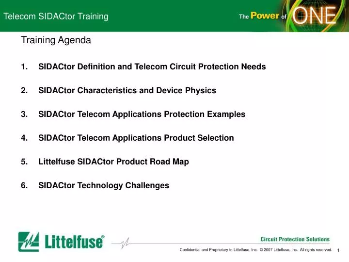
Telecom SIDACtor Training Training Agenda • SIDACtor Definition and Telecom Circuit Protection Needs • SIDACtor Characteristics and Device Physics • SIDACtor Telecom Applications Protection Examples • SIDACtor Telecom Applications Product Selection • Littelfuse SIDACtor Product Road Map • SIDACtor Technology Challenges
Telecom SIDACtor Training Section 1 SIDACtor Definition and Telecom Circuit Protection • SIDACtor Definition • A SIDACtor is a thyristor-based protection device that provides a crowbar current path to protect electronic components/equipment from transient threats • Circuit Protection Needs in Telecom Segment • Lightning • ESD • Inductive • Short Circuit/Power-Cross • SIDACtor Technology for Telecom Overcurrent Circuit Protection • Fast response time • Stable electrical characteristics • Typical Telecom Test Standards • ITU K.20 K.21 • Bellcore GR1089 • UL 60950 • Typical SIDACtor Test Standards • IEEE C62.37 • UL 1449 • UL 1459
SIDACtor Definition and Telecom Circuit Protection SIDACtor Definition • SIDACtor is a thyristor-based protection device that provides a crowbar current path to protect electronic components from transient threats. • The SIDACtor functions: • Bi-directional, voltage-triggered switch • Normally open circuit (high impedance) • Turns on with trigger voltage • On-state becomes low-impedance path • Turns off when current falls below holding level • SIDACtor features as following • Cannot be damaged by transient voltage. • Eliminates the hysteresis and heat dissipation typically found with a clamping device. • Eliminates voltage over-shoot caused by fast rising transients / Extremely fast (<10 ns). • Non-degenerative, will not fatigue / Rugged (Up to 5,000A surge current ratings). • Relatively low capacitance, ideal for high speed transmission equipment.
SIDACtor Definition and Telecom Circuit Protection Circuit Protection Needs in Telecom Systems • Thunderstorms around the world deliver 8 million lightning flashes every day. Peak current in lightning discharges range from a few KA to many hundreds of KA. Induced currents from indirect strikes range from 10A to 20KA. • ESD results from the build up of electrical charge, when two non-conductive materials are brought together then separated. The potential between a human body & an object can exceed 35,000 volts. An ESD event can occur to the telecom system or portable devices through human contact and usage of the telecom devices. • Inductive Load Switching is caused when an inductive load is interrupted. It occurs in factory/industrial environments where motors and relays (inductive loads) are turned on and off. • Short Circuit or Power Cross events can occur due to human error (such cutting a phone and power line simultaneously during construction) or natural disaster such as hurricane, thunderstorm. • One or a combination of the above threats can have obvious adverse effects on semiconductor/IC devices, electro-mechanical contacts, wiring insulation, etc., to cause interruption of telecom equipment operation, telephone service, and even fire.
SIDACtor Definition and Telecom Circuit Protection SIDACtor Technology for Telecom Overvoltage Circuit Protection Telecom equipment should be protected from overvoltage conditions using SIDACtors, GDTs, MOVs, or TVS diodes. • A SIDACtor device is a PNPN device that can be thought of as a TVS diode with a gate. Upon exceeding its peak off-state voltage (VDRM), a SIDACtor device will clamp a transient voltage to within the device's switching voltage (VS) rating. Then, once the current flowing through the SIDACtor device exceeds its switching current, the device will crowbar and simulate a short-circuit condition. When the current flowing through the SIDACtor device is less than the device's holding current (IH), the SIDACtor device will reset and return to its high off-state impedance. • SIDACtor devices are primarily used as the principle overvoltage protector in telecommunications and data communications circuits. Its advantages include: • Fast response time • Stable electrical characteristics • Long term reliability (no wear-out mechanism) • Low capacitance • It is difficult to be damaged by voltage and it has extremely high surge current ratings. • The SIDACtor is a crowbar device, it cannot be used directly across the AC line; it must be placed behind a load. Failing to do so will result in exceeding the SIDACtor device's surge current rating, which may cause the device to enter a permanent short-circuit condition.
SIDACtor Definition and Telecom Circuit Protection Telecom Systems Standards GR 974 GR 1089 K.20 YD/T 1082 NEC 800 UL 497 GR 974 GR 1089 K.21 YD/T 993 NEC 800 UL 497 GR 974 K.20 YD/T 950 UL 497 MDF SLIC GR 1089 K.20 YD/T 950 UL 60950 GR 974 K.20/21 YD/T 950/993 UL 497
SIDACtor Definition and Telecom Circuit Protection SIDACtor Standards • Std C62.37 Specification • Rated parameter values • The values of the rated parameters are established by the manufacturer. • Parameter specifications • Breakover current (IBO) • Breakover voltage (VBO) • Holding current (IH) • Non-repetitive peak on-state current (Itsm) • Non-repetitive peak pulse current (Ipps) • Off-state capacitance (CO) • Off-state (leakage) current (ID) • Off-state voltage (VD) • On-state current (IT) • On-state voltage (VT) • Repetitive peak off-state current (IDRM) • Repetitive peak off-state voltage (VDRM) • Repetitive peak on-state current (ITRM)
Telecom SIDACtor Training Section 2 SIDACtor Characteristics and Device Physics • Basic SIDACtor Characteristics and test procedures • Electrical Characteristics • V-I curve Characteristics • di/dt, dV/dt • Maximum ratings • Continuous / Transient • Thermal Characteristics • Junction Temperature • Signal Integrity Characteristics • Capacitance • SIDACtor Device Physics • SIDACtor Construction and V-I Curve Types • SIDACtor Thermal Effects/Characteristics • SIDACtor Capacitance Effects • SIDACtor Peak Pulse Current
SIDACtor Characteristics and Device Physics V-I Curve and Device Operation In the standby mode, SIDACtor devices exhibit a high off-state impedance, eliminating excessive leakage current and appearing transparent to the circuits they protect. Upon application of a voltage exceeding the switching voltage (VS), SIDACtor devices crowbar and simulate a short circuit condition until the current flowing through the device is either interrupted or drops below the SIDACtor device's holding current (IH). Once this occurs, SIDACtor devices reset and return to their high off-state impedance. VS (Switching Voltage) Maximum voltage prior to switching to on state VDRM (Peak Off-state Voltage) Maximum voltage that can be applied while maintaining off-state VT (On-state Voltage) Maximum voltage measured at rated on-state current. IT (On-state Current ) Maximum rated continuous on- state current IS (Switching Current ) Maximum current required to switch to on-state IH (Holding Current ) Minimum current required to maintain on-state IDRM (Leakage Current ) Maximum peak off-state current measured at VDRM
SIDACtor Characteristics and Device Physics • di/dt Rate of Rise of Current -- Maximum value of the acceptable rate of rise in current over time The purpose of this test is to verify that the SIDACtor can survive a fast rising current, as may occur on the wave front of an impulse. After applying the di/dt impulse to the device, and when it has returned to thermal equilibrium conditions, the device shall not fail any of its specified characteristics. • dV/dt Rate of Rise of Voltage -- rate of applied voltage over time The purpose of this test is to verify that the SIDACtor will not turn on as a result of fast rising system voltages with peak amplitudes lass than the Vdrm rating. A specified voltage ramp equal to the minimum value of critical dv/dt and of amplitude Vdrm shall be applied to the un-energized DUT. The peak ramp voltage shall be maintained for a period of at least 50us. The DUT shall not switch on, even partially, during the test.
SIDACtor Characteristics and Device Physics Maximum Ratings • IPP -- Peak Pulse Current The purpose of this test is to verify that the SIDACtor can survive a specific impulse wave shape of short circuit current amplitude IPP with out failure. The impulse test generator shall be specified for the open-circuit voltage and short-circuit current values, or equivalents, of wave shape and wave shape peak value.
SIDACtor Characteristics and Device Physics Thermal Characteristics • Thermal Resistance The purpose of this test is to determine the continuous power capability of the SIDACtor. Immediately prior to the power being applied, the value of a temperature dependent characteristic shall be measured at the reference temperature. A constant value of power is then applied to the device. Thermal resistance, junction to ambient RөJA = (TJPK - TA) / PTOT °C / W Thermal resistance, junction to case RөJC = (TJPK - TC) / PTOT °C / W Thermal resistance, junction to lead RөJD = (TJPK - TL) / PTOT °C / W Where TA = ambient temperature TC = case temperature TL = lead temperature TJPK = peak junction temperature PTOT = power pulse amplitude
SIDACtor Characteristics and Device Physics Off- State Capacitance • CO The purpose of this test is to determine the off-state capacitance of the SIDACtor under specified conditions. The DUT off-state capacitance, CO, shall be measured at specified dc (VD) and ac (VD and VF) bias levels. In the absence of special requirements, it is recommended that an AC bias level of VD = 0.1 VRMS at a frequency of 100kHz to 1 MHz be used. The DC bias level should be 0 V and any other levels that are representative of the intended application.
SIDACtor Characteristics and Device Physics SIDACtor Construction SIDACtors are manufactured by creating a series of N-type and P-type layers in a silicon chip. The basic thyristor structure has three PN junctions that require four layers (NPNP). The SIDACtor device started manufacture with an N- slice of silicon. Layers of P material are then created at the top and the bottom. A further N+ region is then made on the top surface. Finally the top and the bottom metallization are added to provide contacts. Transistor TR1 is formed by the N+PN- layers. Similarly transistor TR2 is formed by the PN-P layers. The device breakdown voltage is determined by the breakdown of the central N-P layers, which form a shared collector-base junction for TR1 and TR2. The breakdown function is shown as D1. R1 is the lateral resistance of the P layer. R2 together with R1 shunt the base-emitter junction of TR1 to define the value of holding current Ih. R2 has a relatively low value of resistance and is considered as a localized short circuit between base and emitter. During the manufacturing process, the emitter N+ diffusion is perforated with a series of dots to create these short circuits. On the picture, some of the top metallization has been omitted to show the P-type shorting dots.
SIDACtor Characteristics and Device Physics • SIDACtor Types Unidirectional Blocking SIDACtor The inherent (fixed) voltage breakdown can be lowered by gate control, either by use of a single gate or both together. In the non-switching quadrant, current flow will be blocked by the reverse N-P anode junction. Unidirectional Conducting SIDACtor The inherent (fixed) voltage breakdown can be lowered by gate control, either by use of a single gate or both together. In the non-switching quadrant, current flow will be blocked by the reverse PN diode.
SIDACtor Characteristics and Device Physics • SIDACtor Types Bidirectional SIDACtor The inherent (fixed) voltage breakdown can be lowered by controlling the appropriate gate or gates. Bidirectional TRIAC SIDACtor This bidirectional TRIAC has a special gate structure that permits control in both quadrants with a single gate terminal.
SIDACtor Characteristics and Device Physics • SIDACtor Thermal Effects
SIDACtor Characteristics and Device Physics • SIDACtor Thermal Effects
SIDACtor Characteristics and Device Physics SIDACtor Capacitance Effects
SIDACtor Characteristics and Device Physics SIDACtor Non- Repetitive Peak Pulse Current IPP rating can be expressed as specific peak impulse current -time values or with a graph. If the designer ensures that the SIDACtor is always operated below this limiting value, protector failure will not occur.
Telecom SIDACtor Training Section 3 SIDACtor Telecom Applications Protection Examples • Basic Protection Topology • Two Point and Three Terminal Telecom Circuit Protection • Circuit Protection based on Telecom Application Requirement • Customer Premises Equipment • Transformer-Coupled Tip and Ring Circuits • High Speed Transmission Equipment & Interfaces • ADSL • T1/E1 Protection • IDSN • Analog Line Cards • SLIC Protection • Data Line Protection • LAN/WAN Protectors • Littelfuse Global Lab Capabilities • Qualification of Products • UL-Approved Customer Testing • Verification of Standards • Customer Application Testing
SIDACtor Telecom Applications Protection Examples • Basic SIDACtor Topology Two-terminal parallel connected unit Three-terminal parallel and delta connected unit Protector with bridge diodes for wide band systems
SIDACtor Telecom Applications Protection Examples • Primary Protection • Primary protection is provided by the local exchange carrier and can be segregated into three distinct categories as station protection, building entrance protection, and central office (CO) protection. • Protection Requirements • Station protectors must be able to withstand 300A 10x1000 surge events. The building entrance protectors and CO protectors must be able to withstand 100A 10x1000 surge events. It should meet regulatory standards such as UL 497, GR974-CORE and ITU K.28. • Example: Primary Protection Example: Balanced Primary Protection
SIDACtor Telecom Applications Protection Examples • Customer Premises Equipment (CPE) • CPE is defined as any telephone terminal or network equipment which resides at the customer's site and is connected to the Public Switched Telephone Network (PSTN) • Protection Requirements: • CPE should be protected against overvoltages that can exceed 800V and against surge currents up to 100A. It should meet regulatory standards such as TIA -IS-968 and UL 60950 • Example: Basic CPE (Phone, Modem) Protection Application
SIDACtor Telecom Applications Protection Examples • High Speed Transmission Equipment & Interfaces • High speed transmission equipment encompasses a broad range of transmission protocols such as T1/E1, xDSL, and ISDN. Transmission equipment is located at the central office, customer premises, or remote locations. • Protection Requirements: • High speed transmission equipment should be protected against overvoltages that can exceed 2500V and against surge currents up to 500A. It should meet regulatory standards such as TIA -IS-968, GR 1089-CORE, ITU K.20/K.21, and UL 60950 • Example: T1/E1 Protection Application
SIDACtor Telecom Applications Protection Examples • Analog Line Cards • Subscriber Line Interface Cards (SLICs) are highly susceptible to transient voltages that occur at the central office and in remote switching locations. • Protection Requirements • It is often necessary to protect Analog line cards by on-hook (relay) and off-hook (SLIC) protection. It should meet regulatory standards such as TIA -IS-968, GR 1089-CORE, ITU K.20/K.21, and UL 60950. • Example: SLIC Protection
SIDACtor Telecom Applications Protection Examples • Data Line Protection • In many office and industrial locations, data lines such as RS-232, Ethernet, and AC power lines run in close proximity to each other, which often results in voltage spikes being induced onto data lines, possibly causing damage to sensitive equipment. • Protection Requirements • Data lines should be protected against overvoltages that can exceed 1500V and surge currents up to 50A. • Example: 10 Base-T Longitudinal Protection Application
SIDACtor Telecom Applications Protection Examples • Gate Controlled (Programmable) Protection Thyristor (Battrax) Unidirectional gate-controlled protectors Positive and negative gate-controlled protection
SIDACtor Telecom Applications Protection Examples Global Lab Capabilities • Qualification of all LF products • UL-Approved Customer Testing in ISO 17025 Lab (Des Plaines) • High power (AC/DC up to 1KV/50KA) UL approvals available in DP • Telcordia approvals in DP planned (2008) • Verification of Telcordia, ITU, IEC, FCC, and other industry, regulatory, and safety standards • Verification to various OC and OV standards • Insure application meets standards before submitting for approval • Customer Application testing • Assistance with design-in and performance verification • Help with selection of appropriate technology and rating • Application troubleshooting • Assistance insuring proper OV/OC and primary/secondary protection coordination • Competitive evaluations • Competitive or technology performance comparisons • Reliability & Tin Whisker data/testing
Telecom SIDACtor Training Section 4 SIDACtor Telecom Applications Product Selection • SIDACtor Selection • Coordination of Protection • SIDACtor Unique Advantages Over Other Technologies • SIDACtor as a Crowbar Device • SIDACtor Fast Response to Transients • SIDACtor Device Selection • Identify SIDACtor Switching Voltage Requirement • Identify SIDACtor IT Requirement • Identify SIDACtor De-Rating Requirement
SIDACtor Telecom Applications Protection Examples • Coordination of Protection Primary and secondary coordination Coordination among secondary protective devices
SIDACtor Telecom Applications Product Selection Technology SIDACtor GDT MOV TVS Response Time Fastest Slowest Slower response time Fast Capacitance Low As low as 1pF High Higher Current surge rating High As high as 500A for 200 impulses High Low Electrical Characteristic Stable Degrade with time Fatigue after multiple pulses Stable Application Principle over-voltage in telecom, datacom circuit Telecom applications Useful in AC applications Secondary protection • SIDACtor Selection Overvoltage Protection Comparison
SIDACtor Telecom Applications Product Selection • SIDACtor Selection Characteristics of Transient Voltage Suppressor Technology
SIDACtor Telecom Applications Product Selection • SIDACtor Selection
SIDACtor Telecom Applications Product Selection • SIDACtor selection • Off-State Voltage (VDRM) • VDRM of the SIDACtor device must be greater than the maximum operating voltage of the circuit the SIDACtor device is protecting. • POTS (Plain Old Telephone Service) Application: • 150 VRMS (maximum operating voltage) 2 + 56.6 V (maximum DC bias of central office battery) = 268.8 VPK , VDRM > 268.8V • ISDN (Integrated Services Digital Network) Application: • 150 VPK (DC power supply) + 3 VPK (maximum voltage of the transmission signal), VDRM > 153V • Switching Voltage (VS) • The VS of the SIDACtor device should be equal to or less than the peak voltage rating of the component it is protecting • Example 1: VS < Relay Breakdown Voltage • Example 2: VS < SLIC (Subscriber Line Interface Circuit) VPK • Peak Pulse Current (IPP) • The Surge Current Rating (IPP) of the SIDACtor device should be greater than or equal to the surge currents associated with the lightning immunity tests (IPK) • IPP > IPK , IPP >= IPK (Available) : IPK (Available) = VPK/RTOTAL • RTOTAL = RTIP+RSOURCE (Longitudinal) RTOTAL = RTIP +RRING+RSOURCE (Metallic)
SIDACtor Telecom Applications Product Selection • SIDACtor selection • Peak Pulse Current (IPP) • Example 1: Type A surge requirement of TIA/EIA-IS-968(FCC Part 68) with out any series resistance • IPK = 100A, 10x560 us • IPP >= 100A, 10X560 us • We can select "B","C" rated SIDACtor (page 2-4) • Example 2: Surge requirement of GR 1089 with 30 ohm on Tip and 30 ohm on Ring. • IPK = 100A, 10x1000 us • VPK = 1000V, RSOURCE = VPK / IPK = 10 ohm • RTOTAL = RSOURCE + RTIP = 40 ohm • IPK (available) = VPK/RTOTAL = 1000V/40 ohm • IPP >= 25A • Holding Current (IH) • The holding current (IH) of the SIDACtor device must be greater than the DC current that can be supplied during an operational and short circuit condition • Example, TIA/EIA-IS-968 IPK<= 140 mA, IH = 150mA • Off-State Capacitance (CO) • If Insertion Loss is recommended 70% of the original signal value. • Example, Speed >= 30MHz, new MC series is highly recommended.
Telecom SIDACtor Training Section 5 Littelfuse SIDACtor Product Road Map • Teccor Brand • SIDACtor Road Map • Battrax Road Map • Concord Brand • Fixed Voltage Protection Thyristor Road Map • Variable Voltage Protection Thyristor Road Map
Telecom SIDACtor Training Section 6 SIDACtor Technology Challenges • SIDACtor VS and tolerance control • Higher surge ratings and smaller packaging • Multiple devices in one package • SIDACtor technology combined with other technologies in the same package • Improved de-rating characteristics • Higher operating temperatures • Development of programmable SIDACtors • Lead-frame vs. wire-bonding