Download
1 / 18
190 likes | 407 Vues
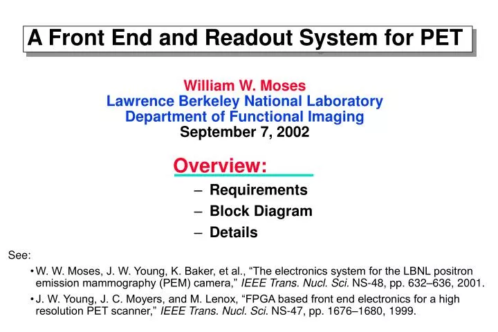
Overview: Requirements Block Diagram Details. A Front End and Readout System for PET . William W. Moses Lawrence Berkeley National Laboratory Department of Functional Imaging September 7, 2002. See:

E N D
Overview: Requirements Block Diagram Details A Front End and Readout System for PET William W. Moses Lawrence Berkeley National Laboratory Department of Functional Imaging September 7, 2002 • See: • W. W. Moses, J. W. Young, K. Baker, et al., “The electronics system for the LBNL positron emission mammography (PEM) camera,” IEEE Trans. Nucl. Sci. NS-48, pp. 632–636, 2001. • J. W. Young, J. C. Moyers, and M. Lenox, “FPGA based front end electronics for a high resolution PET scanner,” IEEE Trans. Nucl. Sci. NS-47, pp. 1676–1680, 1999.
High Rates ~1 MHz Single Event Rate / Detector Module (~500 Modules) ~10 MHz Coincidence Rate Asynchronous Inputs “Coincidence” Data 64 Bit Data from Coinc. End Points of Chord – 107–108 Possible Chords Coincidences Identified using Time Stamp on Singles Events(Arrival Time of Each Gamma Compared to Master Clock) “Singles” Data 24 Bit Data from Single 511 keV Arrival Time – Energy Qualification Crystal ID (Position) – Depth of Interaction? PET Electronics Requirements
Block Diagram: Front End • Module Outputs Processed byAnalog Subsection Board • Analog Subsection Outputs Processed by Detector Head Interface • Output fromDetector Head Interfaceis “Singles Events” • PC/104 Provides Communication toHost PC Based on CTI PET Systems Electronics
Given Analog Signals from 4 PMTs, (1) Generate Digital Data Needed to form (a) “Singles Event Word” or (b) Data Needed for Calibration (2) Send Data to Detector Head Interface Analog Subsection
How Does the Analog Subsection Work? Analog ASIC Discretes Altera FPGA & RAM Condition, Digitize, Process
Analog ASIC Condition (Module Design #1) A B C D X Y Energy CFD A B Adjustable: Gains (4), CFD Settings, Shaping Time, Test Pulse Amplitude D • Analog PMT ASIC Generates Analog: • Timing Strobe (CFD) • Energy Signal (A+B+C+D) • X Signal (B+D-A-C) • Y Signal (A+B-C-D)
Condition (Module Design #2) A B C D X Y Energy CFD PMT Analog ASIC PD Analog ASIC PD Analog Crystal ID (7 bits) • Analog PD ASIC Generates: • Analog Energy Signal • Digital Crystal Address
Energy Signal Digitized with ADC Fixed voltage used as Vref X and Y Ratios Digitized with ADC Energy signal used as Vref input ref ADC input ref ADC input ref ADC Digitize Energy, X Ratio, and Y Ratio X X Ratio (X/E) Y Y Ratio (Y/E) E Energy Vref
TDC Digitizes Time (LSB = ns) Scaler w/ 16 ns clock for MSBs 10 tap delay line (2 ns / tap) w/ latch for LSBs CFD Starts Event Timing Sequence Digitize Time Clock (16 ns) 16 ns Counter t3 t2 t1 CFD Taps Delay Line (2 ns taps) t1 0 0 1 1 1 1 0 0 1 1 1 1 0 0 0 0 t2 Latch t3 1 1 0 0 0 0 1 1
Channel by Channel Gain Correction Channel by Channel Time Correction Compute Crystal Position Performed in Real-Time 256 kB RAM (calibration constants, lookup tables) Calculations done in FPGA Process Result is 24-bit “Singles” Word – Arrival Time – Energy Qualification– Crystal ID (Position) – Depth of Interaction?
Given “Singles Event Words” from Several Analog Subsections, (1) Multiplex & FIFO Them (2) Pass Them To the Coincidence Processor Distributes Control Signals Clock Signals Setup Information Done using FPGAs Detector Head Interface
Block Diagram: Back End • Multiple Detector Heads • One Coincidence Processor • Fiber Optic Link to Data Acquisition PC • PC/104 Loads Set-Up Information intoCoincidence Processor Based on CTI PET Systems Electronics
Given Lots of “Singles Event Words” from the Detector Head Interfaces, (1) Identify Coincident Pairs (2) Compute “Coincidence Event Word” “Coincidence Event Word” is: Chord ID (i.e. location of the 2 crystals) Other Information Dropped(after being used to compute the chord): Time, Depth, Energy Done using FPGAs Coincidence Processor
Collect Singles for Fixed Time (~256 ns) Start with First Single in List Search Later Events for Other Singles Within t (~10 ns) of Its Time If Match, Compute Chord Address Only match geometrically valid pairs Chord computation done by FPGAs Goto Next Single, Loop Until Done How Does Coincidence Processor Work? Lots of Parallel Processing
Easily Programmable Pentium PRO? UNIX Workstation? Controls Runs Type of Run (Real Data or Calibration) Issues “Start” and “Stop” Commands Supervises Data Storage Supervises (or Performs) Reconstruction Computes Calibration Constants Stores and Loads “Setup” Constants Host Computer
Photograph of Components Flex Board & PD ASIC Detector Modules Analog Subsection Detector Head Interface Coincidence Processor
Useful for Compton Camera? • Analog Subsection: • New “Signal Conditioning” ASIC Needed • New (But Similar) Digitization Electronics • New (But Similar) Processing Firmware • Detector Head Interface: • Identical • Coincidence Processor & Host PC: • Identical • Already Scaled to 108 Coincidence Circuits... Definitely!
PET Camera Electronics Consists Of: • Analog Subsection • Detector Head Interface • Coincidence Processor • Host Computer High Rate Capability • 107 Coincident Events per Second(Limited by Detector Dead Time) • Good Energy & Timing Resolution Extensive Use of FPGAs (field programmable gate arrays) •Very Flexible • Algorithms Easily Upgraded & Bugs Fixed • New Logic Can Be Loaded In ~1 Second Eases Testing & Diagnostics Conclusions