Download
1 / 49
1.13k likes | 2.57k Vues
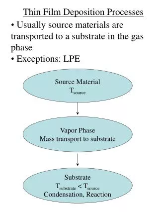
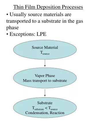
Chapter 9 Thin film deposition. Introduction to thin film deposition. Introduction to chemical vapor deposition (CVD). Atmospheric Pressure Chemical Vapor Deposition (APCVD). Other types of CVD (LPCVD, PECVD, HDPCVD…). Introduction to evaporation.

E N D
Chapter 9 Thin film deposition • Introduction to thin film deposition. • Introduction to chemical vapor deposition (CVD). • Atmospheric Pressure Chemical Vapor Deposition (APCVD). • Other types of CVD (LPCVD, PECVD, HDPCVD…). • Introduction to evaporation. • Evaporation tools and issues, shadow evaporation. • Introduction to sputtering and DC plasma. • Sputtering yield, step coverage, film morphology. • Sputter deposition: reactive, RF, bias, magnetron, collimated, and ion beam. • Deposition methods for thin films in IC fabrication. • Atomic layer deposition (ALD). • Pulsed laser deposition (PLD). • Epitaxy (CVD or vapor phase epitaxy , molecular beam epitaxy). NE 343: Microfabrication and thin film technology Instructor: Bo Cui, ECE, University of Waterloo; http://ece.uwaterloo.ca/~bcui/ Textbook: Silicon VLSI Technology by Plummer, Deal and Griffin
Epitaxial silicon deposition • Advantages of epitaxial wafers over bulk wafers • Offers means of controlling the doping profile (e.g. lightly doped on heavily doped possible) • Epitaxial layers are generally oxygen and carbon free Gases used iin siilliicon epiittaxy
Chemical reactions Concentration o of species at different positions along a horizontal reactor (carrier gas should be H2) SiCl4 + 2H2 Si + 4HCl SiCl4 concentration decreases while the other three constituents (SiHCl3, SiH2Cl2, HCl) increase.
Equipment Three basic reactor configurations • Weight 2000 Kg • Occupy 2m2 or more of floor space. • Quartz reaction chamber with susceptors • Graphite susceptors for physical support. • A coating of silicon carbide (50 to 500 μm) applied by CVD process on susceptors. • RF heating coil or tungsten halogen lamps (cold wall), water cooling.
Si APCVD epitaxy growth process • Hydrogen gas purges of air from the reactor. • Reactor is heated to a temperature. • After thermal equilibrium, an HCl etch takes place at 1150oC and 1200oC for 3 minutes. • Temperature is reduced to growth temperature. • Silicon source and dopant flows are turned on. • After growth, temperature is reduced by shutting off power. • Hydrogen flow replaced by nitrogen flow. • Depending on wafer diameter and reactor type, 10 to 50 wafers per batch can be formed. • Process cycle times are about one hour. • Epitaxy film need high temperature (>1000oC) because at high temperature the (amorphous) native oxide will become unstable and desorb from the surface, exposing the single crystalline silicon lattice for epitaxy.
Arsine doping and growth processes 2AsH3 (gas) 2As (solid) + 3H2 (gas) • Interaction between doping process & growth process • Growth rate influences the amount of dopant incorporated in Si • Equilibrium established at low growth rates. • There is also auto-doping, which can be minimized by: • Fast growth to minimize out-diffusion. • Low temperature deposition reduces boron auto-doping (not As however). • Seal backside of substrate with highly doped poly-oxide. • Avoid the use of HCl etching. • Reduced pressure epitaxy.
Polycrystalline silicon deposition • Application: gate of MOSFET. • Usually deposited in a LPCVD chamber at 25-150Pa, 600-650oC, 10-20nm/min. • SiH4 is preferred because of its lower deposition temperature. H2 carrier gas for solid curves Figure 9-8 • Usually amorphous when deposition at <575oC; but may be polycrystalline if deposition rate is low enough. • Columnar grain structure/texture, and the grain will grow when annealed. • When annealed, amorphous Si will become polycrystalline Si with even large grain size than poly-Si under same annealing. 1Torr = 132 Pa
Grain structure and resistivity Traps states (dopant inactive when trapped there) and scattering at grain boundary limits the resistivity. At higher doping, trap states are all filled and cannot further reduce active dopant concentration.
Deposition rate and oxidation of poly-Si Deposition rate should be pressure since rate ksCG/N for hG>>ks, but actually sub-linear. This is because at higher rate, it is determined by desorption of reaction product H2 (rather than gas transport onto the surface). • Oxidation of poly-silicon: • Usually 900-1000oC dry oxidation. • Un-doped or lightly doped poly-Si oxidizes at rate between that of (111) and (100) single crystal Si. • P-doped poly-Si oxidizes faster than un-doped or lightly doped one.
Silicon nitride deposition • Application: • Masks to prevent oxidation for LOCOS process • Final passivation barrier for moisture and sodium contamination • Etch stop for Cu damascene process • Popular membrane material by Si backside through-wafer wet etch. • PECVD • LPCVD • Can also deposit nitride using silane at 700-900oC by APCVD; or use N2 gas instead of NH3. LPCVD conformal Si3N4films Low-stress nitride deposition using DCS (dichloro-silane SiCl2H2)
Silicon nitride properties tensile or compressive LPCVD film quality is much better than PECVD in almost every aspect.
Silicon dioxide deposition Sputtered oxide has poorer step coverage than CVD. APCVD has been used for many years, but today LPCVD and PECVD are more popular. • Silane based LPCVD • TEOS (tetra-ethoxy-silane). LPCVD 650-800°C, PECVD 350°C. Lower sticking coefficient, thus more conformal film. • Silane based PECVD • Others SiCl2H2 + 2N2O SiO2 + 2N2 + 2HCl (etches Si), 900oC, film contain Cl. TEOS + Ozone (O3). Ozone is more reactive and lowers deposition temperature to 400oC.
Comparison of varied silicon dioxide Lower HF etch rate means better film quality (denser film). For stress, C=compressive, T=tensile
Improve step coverage by PSG reflow No P 2.2% P 4.6% P 7.6% P • Add PH3 to source gas to get P- doped oxide: PSG - phosphosilicate glass • PSG is more flow-able than oxide: reflow at 1000-1100oC to improve step coverage. • Usually 6-8 wt% of P. • Add B can further reduce reflow temperature (BPSG: borophosphosilicate glass)
Deposition of metals MOCVD: metal-organic-CVD
Chapter 9 Thin film deposition • Introduction to thin film deposition. • Introduction to chemical vapor deposition (CVD). • Atmospheric Pressure Chemical Vapor Deposition (APCVD). • Other types of CVD (LPCVD, PECVD, HDPCVD…). • Introduction to evaporation. • Evaporation tools and issues, shadow evaporation. • Introduction to sputtering and DC plasma. • Sputtering yield, step coverage, film morphology. • Sputter deposition: reactive, RF, bias, magnetron, collimated, and ion beam. • Deposition methods for thin films in IC fabrication. • Atomic layer deposition (ALD). • Pulsed laser deposition (PLD). • Epitaxy (CVD or vapor phase epitaxy , molecular beam epitaxy). NE 343: Microfabrication and Thin Film Technology Instructor: Bo Cui, ECE, University of Waterloo, bcui@uwaterloo.ca Textbook: Silicon VLSI Technology by Plummer, Deal, Griffin
Atomic layer deposition (ALD, break CVD into two steps) • Similar in chemistry to CVD, except that the ALD reaction breaks the CVD reaction into two half-reactions, keeping the precursor materials separate during the reaction. • The precursor gas is introduced into the process chamber and produces a monolayer of gas on the wafer surface. A second precursor gas is then introduced into the chamber reacting with the first precursor to produce a monolayer of film on the wafer surface. • Film growth is self-limited (monolayer adsorption/reaction each half-cycle), hence atomic layer thickness control of film growth can be obtained. • That is, one layer per cycle; thus the resulting film thickness may be precisely controlled by the number of deposition cycles. • Two fundamental mechanisms: • Chemi-sorption saturation process • Sequential surface chemical reaction process • Introduced in 1974 by Dr. TuomoSuntola and co-workers in Finland to improve the quality of ZnS films used in electroluminescent displays. • Recently, it turned out that ALD also produces outstanding dielectric layers and attracts semiconductor industries for making High-K dielectric materials.
Example: ALD cycle for Al2O3 deposition 1. Introduce TMA (tri-methyl aluminum) In air, H2O vapor absorb on Si to form Si-O-H. 2. TMA reacts with hydroxyl groups to produce methane.
ALD cycle for Al2O3 deposition 3. Introduce H2O. Reaction product methane is pumped away, leaving an OH- passivation layer on surface. 4. After three cycles. One TMA and one H2O vapor pulse form one cycle. Here 1Å/cycle, each cycle including gas injection and pumping takes few seconds. Two steps each cycle
Closed system chambers (most common) for ALD • The reaction chamber walls are designed to effect the transport of the precursors.
Advantages and disadvantages ALD: slowest, best step coverage • Advantages • Stoichiometric films with large area uniformity and 3D conformality. • Precise thickness control. • Low temperature deposition possible. • Gentle deposition process for sensitive substrates. • Disadvantages • Deposition rate slower than CVD. • Number of different materials that can be deposited is fair compared to MBE.
Chapter 9 Thin film deposition • Introduction to thin film deposition. • Introduction to chemical vapor deposition (CVD). • Atmospheric Pressure Chemical Vapor Deposition (APCVD). • Other types of CVD (LPCVD, PECVD, HDPCVD…). • Introduction to evaporation. • Evaporation tools and issues, shadow evaporation. • Introduction to sputtering and DC plasma. • Sputtering yield, step coverage, film morphology. • Sputter deposition: reactive, RF, bias, magnetron, collimated, and ion beam. • Deposition methods for thin films in IC fabrication. • Atomic layer deposition (ALD). • Pulsed laser deposition (PLD). • Epitaxy (CVD or vapor phase epitaxy , molecular beam epitaxy). NE 343: Microfabrication and Thin Film Technology Instructor: Bo Cui, ECE, University of Waterloo, bcui@uwaterloo.ca Textbook: Silicon VLSI Technology by Plummer, Deal, Griffin
Pulsed laser deposition (PLD) • PLD Characteristics: • Reproduce the composition of the target • Fast response, well controlled deposition rate • Environmentally benign technique • Flexible, easy to implement. • Growth in any environment. • Atoms arrive in bunches. • Uneven coverage. • High defect or particulate concentration. • Not well suited for large-scale film growth. Two targets, co-deposition
Plume generated by laser ablation with different tiny or micro-particles Pulse of fs to ns with peak power high enough (hundreds of MW/cm2) to melt → boil → vaporize → ablate the target surface material, to atoms, ions, electrons, and clusters. Laser Beam Target (b) (c) (d) (a) Plume (plasma) • Laser-material interaction. (a) Absorption and heating; (b) Melting and flowing; (c) Vaporization; (d) Plasma formation in front of the target. Under certain conditions the plasma can detach from the target and propagate toward the laser beam. Substrate Pulse duration < 10 ps Collisionaland multi-photon ionization. Plasma formation without melting. Deviation from 1/2 scaling. Pulse duration > 50 ps Conventional melting, boiling and fracture. Threshold fluence (J/cm2) for ablation scales as 1/2.
PLD physics • Metals, absorption depth 10 nm,depending on wavelength. • Relaxation of energy 1 ps, electron-phonon interaction. • Incredibly non-equilibrium!! • At peak of laser pulse, temperature on target can reach >105 K (> 40 eV!) • Electric field > 105 V/cm, also high magnetic fields • Plasma temperature 3000-5000 K • Ablated species with energy 1–100 eV It is also an excellent micro-machining tool, with clean-cut profile.
Transient plume development 10-6Torr vacuum (plasma of vapor of target material) 100 mTorr O2 (plasma of O2 and vapor of target material) D. Geohegan, Appl. Phys. Lett. 60, 2732 (1992)
Pulsed laser deposition (PLD) system View Windows Excimer laser Chamber Another system
DARPA MICE program (Mesoscopic Integrated Conformal Electronics) • Single (pulsed) laser does surface pretreatment, spatially selective material deposition, surface annealing, component trimming, ablative micromachining, dicing and via-drilling • Direct writing of electronic components- in air! • Rapid process refinement • No masks, pre-forms, or long cycle times • True 3-D structure fabrication possible DARPA: Defense Advanced Research Projects Agency, major US funding agency
Chapter 9 Thin film deposition • Introduction to thin film deposition. • Introduction to chemical vapor deposition (CVD). • Atmospheric Pressure Chemical Vapor Deposition (APCVD). • Other types of CVD (LPCVD, PECVD, HDPCVD…). • Introduction to evaporation. • Evaporation tools and issues, shadow evaporation. • Introduction to sputtering and DC plasma. • Sputtering yield, step coverage, film morphology. • Sputter deposition: reactive, RF, bias, magnetron, collimated, and ion beam. • Deposition methods for thin films in IC fabrication. • Atomic layer deposition (ALD). • Pulsed laser deposition (PLD). • Epitaxy (CVD or vapor phase epitaxy , molecular beam epitaxy). NE 343: Microfabrication and Thin Film Technology Instructor: Bo Cui, ECE, University of Waterloo, bcui@uwaterloo.ca Textbook: Silicon VLSI Technology by Plummer, Deal, Griffin
Introduction • Epitaxy refers to the method of depositing a monocrystalline film on a monocrystalline substrate. • The word “epitaxy” comes from the Greek for ‘above’ (epi) and ‘in an ordered manner’ (taxis): to arrange upon. • Autoepitaxy(or Homoepitaxy): extension of the substrate lattice by the overgrowth of a layer of identical material (e.g. Si on Si or GaAs on GaAs) with no problem of compatibility or mismatch. • Heteroepitaxy: any two materials of different crystalline structure and orientation (e.g. (001) GaAs on (001) Si or (001) Si on Sapphire) Epilayer Epitaxy Initial substrate 33 Most slides in this section prepared by EhsanFathi
Heteroepitaxyconditions • Heteroepitaxy Conditions: • Substrate must be physically and chemically inert to the growth environment and being prepared with a damage-free surface. • Chemical compatibility between the materials to avoid compound formation or massive dissolution of one layer by the other. • Matched thermal expansion characteristics between the layer and substrate to avoid excess stress upon cooling → formation of dislocation at the interface, or even breaking of the structure • Matched lattice parameters between the layer and substrate → not a serious problem 34
Strained and unstrained Schematic illustration of (a) lattice-matched, (b) strained, and (c) relaxed hetero-epitaxial structures. Homoepitaxy is structurally identical to the lattice-matched heteroepitaxy. 35
Strained and unstrained • Experimentally determined critical layer thickness for defect-free, strained-layer epitaxy of GexSi1-x on Si, and Ga1-xInxAs on GaAs. 36
Strained-layer superlattices • Strained-layer superlattices : in some devices we need repeated, regular alternation between two monocrystalline • With these structures we can alter the basic physical properties of the material • Because the layers are sufficiently thin, the lattice mismatch is accommodated by uniform strains in the layers. • The new lattice will have an equilibrium lattice constant b such that a1 > b > a2 (for a1 > a2) direction of the strain 37
Growth methods • Vapor-Phase Epitaxy (VPE, a form of CVD):transport of the epilayer constituents (Si, Ga, As, dopants,…) in the form of one or more volatile compounds to the substrate where they react to form the epilayer. • Molecular Beam Epitaxy: physical transport of material to a heated substrate through vacuum evaporation. • Liquid-Phase Epitaxy (LPE): the growth of epitaxial layer on crystalline substrate by direct precipitation from the liquid phase. 38
Silicon VPE • SiCl4, SiH2Cl2, SiHCl3, and SiH4 have been used for VPE growth. • Silicon tetrachloride is the most studied and has the widest industrial use. • Other silicon sources are used because of lower reaction temperature. @ 1200 oC • An additional competing reaction is taking place: • If the silicon tetrachloride concentration is too high, etching rather than growth of silicon will take place. • If the carrier gas entering the reactor contains hydrochloric acid, etching will take place. • This etching is used for in-situ cleaning of the Si wafer prior to epitaxial growth. 39
The halide process for GaAs deposition • In this process transport of gallium accomplished by means of the halide, AsCl3. • Both hydrogen and AsCl3 vapor enter the system and they react: • This reaction product flow over the gallium source and GaAs formed as a crust on the surface of gallium • The HCl gas resulting from the first reaction transfer gallium to the substrate in the form of GaCl, where the GaAs is deposited @ 750 oC: 40 Should be fully saturated with As
The hydride process for GaAs deposition • Fluxes of gallium and arsenic species formed independently → greater control in the vapor phase, and hence a wider control of the deposition parameters • As4 for As, and gallium chloride (GaCl) for Ga component are used. • As4 is generated by thermal decomposition of arsine (AsH3): • Gallium chloride is generated by the reaction: For In-situ etching 41
The organometallic process MOCVD: metal-organic CVD = OMVPE: organo-metallic vapor phase epitaxy • Halide and hydride processes cannot be extended to the growth of AlGaAs by the simultaneous growth of GaAs and AlAs ( growth of AlAs occurs ~ 1100oC). • This problem avoided in the organometalic process. • Many materials that we wish to deposit have very low vapor pressures and thus are difficult to transport via gases. • One solution is to chemically attach the metal (Ga, Al, Cu, etc…) to an organic compound that has a very high vapor pressure. • • The organic-metal bond is very weak and can be broken via thermal means on wafer, depositing the metal with the high vapor pressure organic being pumped away. Some MOCVD precursor gases: Tri-methyl-aluminum, liquid Tri-methyl-gallium, liquid Arsine AsH3, gas Di-methyl selenide, liquid Di-methyl zinc, liquid http://en.wikipedia.org/wiki/Metalorganic_vapour_phase_epitaxy 42
The organometallic process Advantages: Highly flexible → we can deposit semiconductors, metals, dielectrics Disadvantages: Highly toxic, very expensive source material, and environmental disposal costs are high. Material deposited: III-V semiconductors - AlGaAs, AlGaInP, AlGaN, AlGaP, GaAsP, GaAs, GaN, GaP, InAlAs, InAlP, InSb , InGaN, GaInAlAs, GaInAlN, GaInAsN, GaInAsP, GaInAs, GaInP, InN, InP. II-VI semiconductors - Zinc selenide (ZnSe), HgCdTe, ZnO, Zinc sulfide (ZnS) IV semiconductors - Si, Ge, strained silicon 43
Molecular-beam epitaxy (MBE) • MBE is an epitaxial process involving the reaction of one or more thermal beams of atoms or molecules with a crystalline surface under UHV conditions. • Precise control in both chemical composition and doping profiles. • It has a very low growth rate (e.g. for GaAs, a value of 1μm/hr is typical.) • Single-crystal multilayer structures with dimensions on the order of atomic layers can be made. Diagnostic tools 44
Effusion cell (Knudsen cell) • The most common type of MBE source is the effusion cell. Sources of this type are sometimes called Knudsen, or K-cells. • The crucible and source material are heated by radiation from a resistively heated filament. A thermocouple is used to allow closed-loop feedback control. • A typical Knudsen cell contains a crucible (made of pyrolytic boron nitride (PBN), quartz, tungsten or graphite), heating filaments (often made of metal tantalum), water cooling system, heat shields and shutter. • PBN crucible • Resistive heater filament • 3. Metal foil radiation shields • 4. Thermocouple • 5. Mounting flange 45
RHEED • Reflection high-energy electron diffraction (RHEED) is a technique used to characterize the surface of crystalline materials. • A RHEED system consist of an electron source (gun), and a photoluminescent detector screen. • The electron gun generates a beam of electrons which strike the sample at a very small angle relative to the sample surface. • Incident electrons diffract from atoms at the surface of the sample, interfere constructively at specific angles and form regular patterns. 46
RHEED • The 3D surface results in a spotty pattern due to the electron transmission through surface roughness. • The more 2D surface giving rise to the commonly observed RHEED streaks. 47
MBE system 48
Liquid-phase epitaxy (LPE) • LPE involves the growth of epitaxial layers on crystalline substrate by direct precipitation from the liquid phase. • In LPE, the substrate is held in contact with the supersaturated solution (As saturated solution of Ga). • Cooling the arsenic saturated solution of gallium causes the arsenic to precipitate in the form of GaAs. • Typical deposition rates for monocrystalline films range from 0.1 to 1 μm/min. • LPE in most cases is a very economic deposition techniques, especially when up-scaled to mass-production 49