Download
1 / 58
770 likes | 2.26k Vues
Ductile-Regime Machining of Silicon Carbide and Quartz. by Deepak Ravindra Thesis Defense (Mechanical Engineering) Thesis Advisor: Dr. John A. Patten . Presentation Overview. Introduction Research Background 4 projects Ductile to Brittle Transition (DBT) of 4H-SiC

E N D
Ductile-Regime Machining of Silicon Carbide and Quartz by Deepak Ravindra Thesis Defense (Mechanical Engineering) Thesis Advisor: Dr. John A. Patten
Presentation Overview • Introduction • Research Background • 4 projects • Ductile to Brittle Transition (DBT) of 4H-SiC • Single point diamond turning (SPDT) of CVD-SiC • Hybrid laser-SPDT process for CVD-SiC • SPDT of Quartz • Future/Upcoming work • Acknowledgements
Ductile Regime Machining Plastic flow of material in the form of severely sheared machining chips occur Possible due to High Pressure Phase Transformation (HPPT) or direct amorphization Plastic deformation caused from highly localized contact pressure and shear stresses. High pressure (metallic) phase could be used to improve manufacturing processes and ductile response during machining.
Ductile Regime Machining of Ceramics • Model proposed by Blake and Scattergood • DBT is calculated based on material properties • Depth exceeding critical depth will result in brittle machining • Micro-cracks / surface damage depth, yc should not extend beyond the cut surface plane
Critical Depth of Cut (dc) • Griffith fracture propagation criteria: dc ~ 0.15 . (E / H) . (Kc / H)2 where: 0.15 = estimated constant of proportionality E = elastic modulus H = hardness Kc = fracture toughness
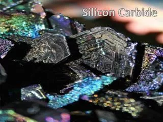
Why Use Silicon Carbide? Extreme hardness (~27GPa for Polycrystalline CVD coated) High wear resistance High thermal conductivity (3.4 W/cm.K)* High Temperature Operation Wide energy bandgap (3.26eV)* High electric field breakdown strength (2.22 x 10⁶ V/cm)* High maximum current density High saturated electron drift velocity (2 x 107 cm/sec)* *Values for 4H single-crystal
Project I –Ductile to Brittle Transition (DBT) of a 4H Single Crystal SiC Wafer by Performing Nanometric Machining
Applications of 4H SiC High-Frequency Power Devices RF & Microwave Amplifiers/Transmitters High-Temperature Devices High temperature electronics & power devices Optoelectronic Devices Laser diodes & photodiodes III-V Nitride Deposition Light emitting devices
Experimental Plan • 3 depth of cuts (100nm, 500nm & 1000nm) were planned to be carried out using the Nanocut II • Predicted range of Ductile to Brittle Transition (DBT) is between 100nm – 1000nm (based on calculations and previous experiments) • A depth greater than 1000nm will only be carried out if the DBT is not identified with the first set of experiments. • Cuts will be imaged and analyzed using the AFM
Experimental Method-Nanocut II Z-axis Force Sensor Diamond Tool PZT Tube & Cap Gage X-axis Force Sensor Sample Mount Figure 1
3”(76.2mm) SiC wafer (4H-Single Crystal) The primary flat is the {1010} plane with the flat face parallel to the <1120> direction. The primary flat is oriented such that the chord is parallel with a specified low index crystal plane. The cutting direction is along the <1010> direction Figure 2
Nanocut matrix of cuts The cuts were done in array pattern to help with imaging Figure 3
Results – Actual Cuts on SiC Cuts image under an optical microscope at 400x magnification Dimensions are approximately 10-20µm in length and 120µm in width Cutting direction from right to left The 10mm tool nose radius makes the cuts wider than they are longer The maximum depth of cut is at the middle of the cut Figure 4
Results- Force Data Cutting and thrust forces increase as the depth of cut increases The cutting forces are consistently greater than the thrust forces for all depths The force data does not indicate direct evidence of a DBT Beyond the DBT, the force data may indicate brittle fracture Less energy/force required to fracture material compared to ductile response. In this case, the brittle fracture was not so severe as to measurably affect the resultant force trends Figure 5
Results- Height Profile (Ductile) An AFM scanned section of a (1000nm programmed depth) cut. All the 100nm & 500nm depth of cuts were completely ductile The measured depth is 816nm. The “V” shape of the ductile cut represents the imprint of the tool Cutting Direction Figure 6
Cutting Direction Results- Height Profile (DBT) An AFM scanned section of a cut where the brittle characteristic of the material is visible. The measured depth is 836nm. Figure 7
Results- Height Profile (Brittle) Cutting Direction • The maximum measured depth of cut (1170nm) is more than the programmed depth of cut (1000nm). • Due to microcracks that could extend deeper than the depth of cut below the machined surface Figure 9
Cutting Direction Results – Brittle Cut Optical image (200x) of 1000nm cut showing brittle fracture Jagged edges are due to crack propagation and uncontrolled material removal in the brittle regime. Figure 10
Ra Figure 11 Results – Brittle Cut Cutting Direction White light interferometric microscope (WYKO) image of 1000nm brittle cut The actual depth varies from zero at the ends (top and bottom of the cuts, outside the field of view) to a maximum in the middle.
Conclusion The DBT depth for a 4H-SiC wafer was determined to be between 820nm-830nm in the <1010> cutting direction. Cutting forces and thrust forces increase as the depth of cut increases Beyond the DBT depth, the cut produced becomes brittle The fracture from brittle cutting then leads to pitting and microcracks, this results in significant and uncontrolled subsurface damage In order to machine a semiconductor or ceramic in the ductile-regime, it is crucial to know its DBT depth
Project Goals (common for the three SPDT experiments) • Improve surface finish (surface roughness) via ductile mode machining • Increase material removal rate (MRR) by altering: • Feed • Depth of Cut • Cutting Speed • Minimize diamond tool wear *Establish machining parameters to meet all three criteria's (project goals)
Project II - Improving the Surface Roughness of a CVD-SiC by Performing Ductile Regime SPDT • 6” disk from POCO Graphite Inc. was used • Mirror finish surface required • To be used as optic mirrors in an Airborne Laser (ABL) device • CVD coated SiC is preferred because: • High Purity (>99.9995%) • High Density (99.9%) • Homogeneity • Chemical & Oxidation Resistance • Good Cleanability & Polishability • Good Thermal & Dimensional Stability
Experimental Procedure • Initial test matrix is design (with varying depths of cuts and feeds) • Preparatory machining on 2” polished CVD-SiC • Preliminary machining on 6” CVD-SiC (as-received) • Final experimental matrix is designed based on preparatory and preliminary machining results • Final machining on 6” CVD-SiC
Results (surface roughness & feed correlation) • Data is arranged from highest to lowest feed • Feed is more dominant than depth of cut when improving surface roughness • Feed is reduced when surface roughness does not improve
Results (Rz for all machining passes) • The Rz value was used to determine the required depth of cut • The feed and/or depth of cut is reduced when the Rz value does not improve.
Results (Cutting force vs. depth of cut) • Depth of cut, feed and surface roughness influence the cutting forces • Depth of cut is the dominant parameter
Results (Surface image of 6 passes) • Image was taken at 50x magnification • Surface continuously improved after each pass • Band between pass 4 & 5 was due to tool chatter
Results (Surface image comparison) • Images comparing the surface before (left) and after (right) SPDT • Images were taken at a 1000x magnification • The sharp/uneven peaks on the surface disappeared after the SPDT operation
Results (SEM images of tool wear) • Tool was used for pass 1 (2µm depth & 30µm/rev feed) • SEM images are used to measure tool wear • Wear length across cutting edge • Rake wear • Flank wear
Results (Cutting force vs. tool wear across cutting edge) • Wear across cutting edge radius is a function of depth of cut • Wear length and cutting forces increase as depth of cut increases
Conclusion • Recommended machining parameters for commercial manufacturing of CVD-SiC • Best surface finish is achieved from the lowest feed • Tool wear can be minimized by using cutting fluids
Project III-Developing a Hybrid Laser-SPDT Machining Process for Smoothing Ceramics • To develop a more efficient manufacturing process of SiC • Laser machining done by Mound Laser & Photonics Center (MLPC) using a pico-second pulsed laser
Images of CVD-SiC Samples • All plateaus were laser machined using different ablation parameters • These plateaus were then diamond turned at a 1µm depth with a 1µm/rev feed.
Results (Surface roughness) • Data is arranged from the roughest to the smoothest as-received plateau • The Ra values dropped by almost 50% after just a single pass
Results (tool wear vs. track length) • The longer the track length, the more the measured tool wear across the cutting edge radius
Results (tool wear vs. track length) • The longer the track length, the more the measured rake & flank wear • Flank wear > Rake Wear
Results (surface roughness comparing 1µm/rev & 5µm/rev feeds) • A second set of experiments were carried out to extend the tool life • Changing the feed did not affect the surface roughness data significantly
Results (tool wear data comparing 1µm/rev & 5µm/rev feeds) • Life of tool was extended by increasing the feed (due to shorter track length)
Conclusion • The 60-1 laser ablated sample proved to be the best combination for SPDT • This combination yielded in low surface roughness, low cutting force and longer track length.
Project IV – Machining & Improving the Surface Roughness of Quartz by SPDT • Advantages of Quartz: • High hardness (~9.8GPa) • Large supply (most abundant non-metallic mineral on earth) • Good optical properties (optical range from 180nm to 2000nm) • Goal of the experiment: • Obtain surface roughness (Ra) lesser than 50nm • Predict tool wear and other machining parameters to be able to diamond turn a 14” quartz
Use of final 14” disk • To be used as ABL device nose cover • Mirror finish surface required for the above use • Image courtesy of Boeing Corporation
Experimental Plan • Preparatory machining will be conducted to: • To confirm that ductile regime SPDT can be carried out • Correlate the trust force and depth of cut • Adjust sample runout for force/machining stability • Observe tool wear • Final machining experiment (if preparatory experiments are successful)
Results (preparatory exp.) • Image of surface shows no signs for cracks/fracture • Feed marks seen on machined region • Tool showed no significant wear
Results (preparatory exp. machining chips) • Continuous plastically deformed chips indicate ductile mode machining. • Both images were taken at a 400x magnification