Download
1 / 27
270 likes | 461 Vues
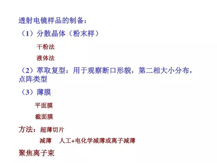
透射电镜样品的制备: ( 1 )分散晶体(粉末样) 干粉法 液体法 ( 2 )萃取复型:用于观察断口形貌,第二相大小分布,点阵类型 ( 3 )薄膜 平面膜 截面膜 方法: 超薄切片 减薄 人工 + 电化学减薄或离子减薄 聚焦离子束. 选区电子衍射:. 阿贝衍射原理. 220. 010. 110. g 110. b*. a*. 000. 100. 倒易点阵与正点阵. g 110. r 110. b. a. d 110. S / l = k.

E N D
透射电镜样品的制备: (1)分散晶体(粉末样) 干粉法 液体法 (2)萃取复型:用于观察断口形貌,第二相大小分布,点阵类型 (3)薄膜 平面膜 截面膜 方法:超薄切片 减薄 人工+电化学减薄或离子减薄 聚焦离子束
选区电子衍射: 阿贝衍射原理
220 010 110 g110 b* a* 000 100 倒易点阵与正点阵 g110 r110 b a d110
S/l= k S0/l= k0 ghkl 衍射几何条件:厄瓦球面
(hkl) S/l= k S0/l= k0 L=相机长度 ghkl (hkl) 000 The size of diffraction patterns q (1/l)/ghkl=L/Rhkl’ R’d = lL When is q small (electron diffraction), Rd=lL=diffraction constant Rhkl ’ Rhkl
图3.9 Al3Ni 型正交相Al74.8Fe1.5Ni23.7的选区电子衍射花样 (hkl) Plotting and indexing of single crystal spot patterns S/l= k S0/l= k0 相机长度 ghkl 000 When q is small (electron diffraction), the reflection sphere cuts a 2D reciprocal plane. Rhkl
(hkl) Plotting and indexing of single crystal spot patterns S/l= k S0/l= k0 相机长度 ghkl 000 Indexing: the plane normal [uvw] and at least one low index spot (hkl) (normally two spots), with hu+kv+lw=0. Rhkl
(hkl) Plotting and indexing of single crystal spot patterns S/l= k S0/l= k0 相机长度 ghkl 000 For a known substance but unknown orientation, a table of interplanar spacings d is needed. a) Choose three spots such as h3k3l3, h1k1l1, h2k2l2. b) Measure the d values, and thus determine the indices. c) By trial and error a consistent set of indices is chosen such that h3k3l3= h1k1l1 + h2k2l2. d) [uvw], the zone axis, is obtained by any two vectors (e.g. R1×R2) Rhkl h3k3l3 h1k1l1 h2k2l2 R2 R1 [uvw]
002 111 111 [110] Plotting and indexing of single crystal spot patterns Example: an fcc crystal with a = 0.58nm. d=a/(h2 +k2 +l2)1/2. A diffraction pattern is shown below with R1=R2=8.96mm, R1^R2=109.5º. Ll=3.0 nm.mm. a) Choose three spots R1, R2, R3 (R3 = R1 + R2 ) b) d1= d2= Ll/R1= 0.335nm, {111}. c) A consistent set of indices is 002= 111 + -1-11. d) R1×R2=[1-10], the zone axis晶带轴. R3 也可以直接查表 R2 R1 109.5º
PARAMETERS A= 5.8000 B= 5.8000 C= 5.8000 Å AF= 90.000 BT= 90.000 GM= 90.000 NUVW= 3 NSY= 1 NL= 1 SY: 1-CUBIC; 2-TETRA; 3-ORTH; 4-HEX; 5-MONO; 6-TRIC LT: 1-F; 2-I; 3-C; 4-B; 5-A; 6-P; 7-R; K U V W H1 K1 L1 H2 K2 L2 R2/R1 R3/R1 FAI d1 d2 1 1 1 1 0 2 -2 -2 0 2 1.000 1.000 120.00 2.051 2.051 2 1 1 0 -1 1 -1 -1 1 1 1.000 1.155 70.53 3.349 3.349 3 1 0 0 0 -2 0 0 0 -2 1.000 1.414 90.00 2.900 2.900 4 3 3 2 2 -2 0 1 1 -3 1.173 1.541 90.00 2.051 1.749 5 2 2 1 2 -2 0 0 2 -4 1.581 1.581 108.43 2.051 1.297 6 2 1 1 1 -1 -1 0 2 -2 1.633 1.915 90.00 3.349 2.051 7 3 1 0 0 0 -2 -1 3 -1 1.658 1.658 72.45 2.900 1.749 8 3 1 1 0 -2 2 2 -4 -2 1.732 1.732 73.22 2.051 1.184 9 3 2 2 0 2 -2 -4 2 4 2.121 2.121 103.63 2.051 .967 10 3 3 1 2 -2 0 2 0 -6 2.236 2.236 77.08 2.051 .917 11 2 1 0 0 0 -2 -2 4 0 2.236 2.449 90.00 2.900 1.297 12 3 2 1 1 -1 -1 -1 3 -3 2.517 2.582 97.61 3.349 1.331 13 3 2 0 0 0 -2 -4 6 0 3.606 3.742 90.00 2.900 .804 002 111 R2 220 R3 R1 109.5º 111 [110]
Indexing of single crystal spot patterns from an unknown phase Procedure Survey the literature to collect information of possible phases. Three possible routes to reach its full indexing Calculate d spacings and compare with standard powder XRD data; Measure R2/R1, R2^R1, and compare with tables in archives; Try a cubic phase; Use double tilting to determine directly the 3D reciprocal lattice. In general three independent patterns are necessary to determine a reciprocal structure. R3 A diffraction pattern is shown on the right: R1=R2=14.4mm, R1^R2=109.5º. Ll=3.0 nm*mm. R2 R1 109.5º
d1=d2 0.208 d3= 0.180 d4= 0.127 Standard powder XRD data;
Cubic indexing Cubic indexing Choose three shortest reciprocal vectors R1, R2, R3, R3=R1+R2, measure the angle R1^R2. Calculate d1, d2, (R2/R1)2, (R3/R1)2. Judge possible combinations of hkl. In general three independent patterns are necessary to determine the reciprocal structure. A diffraction pattern is shown on the right: R1=R2=14.4mm, R1^R2=109.5º. Ll=3.0 nm*mm. R3 R2 R1 d1 d2 (R2/R1)2 (R3/R1)2 0.208 0.208 1 (1.155)2=4/3 109.5º
h2+k2+l2 (hkl) 简单立方 体心立方 面心立方 1 100 100 2 110 110 110 3 111 111 111 4 200 200 200 200 5 210 210 6 211 211 211 8 220 220 220 220 Cubic indexing R1=R2=14.4mm, R1^R2=109.5º. Ll=3.0 nm*mm. R3 d1 d2 (R2/R1)2 (R3/R1)2 0.208 0.208 1 (1.155)2=4/3=8/6 111 111 111/111 002/111 R2 R1 109.5º
002 111 111 [110] Cubic indexing Self-consistency of indices: (111)+ (-1-11)=(002) Angle check: (111)^(-1-11)=109.5º Lattice constant check: a=d111*3=0.360 nm Two more patterns are necessary to assure the phase identification R1=R2=14.4mm, R1^R2=109.5º. Ll=3.0 nm*mm. R3 d1 d2 (R2/R1)2 (R3/R1)2 0.208 0.208 1 (1.155)2=4/3 111 -1-11 -1-11/111 002/111 cF, a = 0.36 nm.奥氏体铁 R2 R1 109.5º
Exercises: index the following patterns in cubic schemes. Note that there may be more than one possibilities for each patterns. Give the corresponding lattice types and constants. R3 R2 R1 [111] R1= R2= R3= 23.6mm, R1^R2=120º. Ll=3.0 nm*mm. d1 d2 (R2/R1)2 (R3/R1)2 lattice constant 0.127 0.127 1 1 110 -101 -101/110 011/110 cP, cI 0.18 nm 220 -202 -202/220 022/220 cF 0.36 nm
Exercises: index the following patterns in cubic schemes. Note that there may be more than one possibilities for each patterns. Give the corresponding lattice types and constants. R2 R3 R1 [001] R1= R2= 16.7mm, R1^R2=90º. Ll=3.0 nm*mm. d1 d2 (R2/R1)2 (R3/R1)2 lattice constant 0.180 0.180 1 1 100 010 010/100 110/100 0.180 nm 1-10 110 110/1-10 200/1-10 0.255 nm 200 020 020/200 220/200 0.360 nm
Exercises: index the following patterns in cubic schemes. Note that there may be more than one possibilities for each patterns. Give the corresponding lattice types and constant. R1 R3 R2 [130] R1= 16.7 mm, R2 = R3= 27.5 mm, R1^R2=107.5º. Ll=3.0 nm*mm. d1 d2 (R2/R1)2 (R3/R1)2 0.180 0.109 11/4 11/4 002 -31-1 -31-1/002 -311/002 cF, 0.36 nm
Exercises: index the following patterns in cubic schemes. Note that there may be more than one possibilities for each patterns. Give the corresponding lattice types and constants. R1 R3 R2 [110] R1= 16.7mm, R2=23.6 mm, R1^R2=90º. Ll=3.0 nm*mm. d1 d2 (R2/R1)2 (R3/R1)2 a 0.180 0.127 2 3 001 -110 -110/001 -111 /001 cP 0.18 nm 1-10 002 002/1-10 1-12/1-10 cI 0.255 nm 002 -220 -220/002 -222/002 ×
a1 a1 a3 a3 a2 a2 Use double tilting to determine directly a 3D reciprocal lattice 000 000
001 [100] 000 [001] 010 a1=26.56 010 a1 001 [210] a3 a2 120 100 120 110 a2=18.43 111 001 [110] 110 a3=18.43 101 001 [010] 000 100
图3.4 六角相Al5FeNi的选区电子衍射花样 Figure 3.4 SAED patterns arranged in a stereo manner of the hexagonal Al5FeNi phase. Use double tilting to determine directly a 3D reciprocal lattice
Ring patterns For randomly orientated aggregates of polycrystals, the reciprocal lattice becomes a series of spheres. The radii Ri = Ll/di. The number of points contributing to each sphere is known as the multiplicity.
Ring patterns 典型非晶电子衍射
图3.5 铸态合金Al71Fe5Ni24的X 射线(λCuK= 0.15406 nm)衍射谱 Figure 3.5 X-ray diffraction pattern of the as-cast Al71Fe5Ni24 alloy. Powder patterns
Ring patterns • How to index a known powder pattern • Calculate the d list • Find out the indices for each peak • How to index an unknown powder pattern • Survey the literature • Calculate the d list • Compare with XRD cards