Download
1 / 20
270 likes | 755 Vues
Lecture 08: Pass Transistor Logic. NMOS Transistors in Series/Parallel. Primary inputs drive both gate and source/drain terminals NMOS switch closes when the gate input is high Remember - NMOS transistors pass a strong 0 but a weak 1. A. B. X = Y if A and B. X. Y. A.

E N D
NMOS Transistors in Series/Parallel • Primary inputs drive both gate and source/drain terminals • NMOS switch closes when the gate input is high • Remember - NMOS transistors pass a strong 0 but a weak 1 A B X = Y if A and B X Y A X = Y if A or B B X Y
PMOS Transistors in Series/Parallel • Primary inputs drive both gate and source/drain terminals • PMOS switch closes when the gate input is low • Remember - PMOS transistors pass a strong 1 but a weak 0 A B X = Y if A and B = A + B X Y A X = Y if A or B = A B B X Y
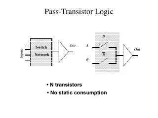
Pass Transistor (PT) Logic B B A A F = A B B B F = A B 0 0 • Gate is static – a low-impedance path exists to both supply rails under all circumstances • N transistors instead of 2N • No static power consumption • Ratioless • Bidirectional (versus undirectional)
B VTC of PT AND Gate B 1.5/0.25 B=VDD, A=0VDD 0.5/0.25 Vout, V A 0.5/0.25 A=VDD, B=0VDD A=B=0VDD F = AB 0 0.5/0.25 Vin, V • Pure PT logic is not regenerative - the signal gradually degrades after passing through a number of PTs (can fix with static CMOS inverter insertion)
A A A A A A B B B B B B B B B B A A A F=A+B F=AB F=AB B B F=A+B F=AB F=AB A OR/NOR XOR/XNOR AND/NAND Differential PT Logic (CPL) A PT Network F B F A Inverse PT Network F F B
CPL Properties • Differential so complementary data inputs and outputs are always available (so don’t need extra inverters) • Still static, since the output defining nodes are always tied to VDD or GND through a low resistance path • Design is modular; all gates use the same topology, only the inputs are permuted. • Simple XOR makes it attractive for structures like adders • Fast (assuming number of transistors in series is small) • Additional routing overhead for complementary signals • Still have static power dissipation problems
A A Cin Cin B B B Cin CPL Full Adder Cin B A !Sum Sum B Cin A !Cout B Cin Cout
VGS NMOS Only PT Driving an Inverter • Vx does not pull up to VDD, but VDD – VTn In = VDD Vx = VDD-VTn M2 A = VDD D S B M1 • Threshold voltage drop causes static power consumption (M2 may be weakly conducting forming a path from VDD to GND) • Notice VTn increases of pass transistor due to body effect (VSB)
Voltage Swing of PT Driving an Inverter • Body effect – large VSB at x - when pulling high (B is tied to GND and S charged up close to VDD) • So the voltage drop is even worse Vx = VDD - (VTn0 + ((|2f| + Vx) - |2f|)) In In = 0 VDD 1.5/0.25 x = 1.8V x D S VDD Out Voltage, V 0.5/0.25 B 0.5/0.25 Out Time, ns
Cascaded NMOS Only PTs B = VDD B = VDD C = VDD G x y Out A = VDD M1 M2 A = VDD M1 x = VDD - VTn1 S G y Out C = VDD M2 S Swing on y = VDD - VTn1 - VTn2 Swing on y = VDD - VTn1 • Pass transistor gates should never be cascaded as on the left • Logic on the right suffers from static power dissipation and reduced noise margins
Level Restorer on Mr off B Out=0 A=1 M2 x = 0 A=0 Mn Out =1 1 M1 Solution 1: Level Restorer • For correct operation Mr must be sized correctly (ratioed) • Full swing on x (due to Level Restorer) so no static power consumption by inverter • No static backward current path through Level Restorer and PT since Restorer is only active when A is high
Transient Level Restorer Circuit Response W/L2=1.50/0.25 W/Ln=0.50/0.25 W/L1=0.50/0.25 node x never goes below VM of inverter so output never switches W/Lr=1.75/0.25 Voltage, V W/Lr=1.50/0.25 W/Lr=1.25/0.25 W/Lr=1.0/0.25 Time, ps • Restorer has speed and power impacts: increases the capacitance at x, slowing down the gate; increases tr (but decreases tf)
Solution 2: Multiple VT Transistors • Technology solution: Use (near) zero VT devices for the NMOS PTs to eliminate most of the threshold drop (body effect still in force preventing full swing to VDD) low VT transistors In2 = 0V A= 2.5V on Out off but leaking B= 0V In1 = 2.5V sneak path • Impacts static power consumption due to subthreshold currents flowing through the PTs (even if VGS is below VT)
C C Solution 3: Transmission Gates (TGs) • Most widely used solution • Full swingbidirectional switch controlled by the gate signal C, A = B if C = 1 A B A B C C C = GND C = GND A = VDD B A = GND B C = VDD C = VDD
Resistance of TG W/Lp=0.50/0.25 0V Rn Rp 2.5V Vout Rp Rn Resistance, k 2.5V Req W/Ln=0.50/0.25 Vout, V
S S TG Multiplexer S F S VDD In2 S F In1 S GND F = !(In1 S + In2 S) In1 In2 S
Transmission Gate XOR weak 0 if !A off on A !B A A B off on B !A weak 1 if A 0 B an inverter 1
Cin B A Sum Cout TG Full Adder
A A A A A B B B B B Differential TG Logic (DPL) B A B A A A F=AB F=AB GND B B GND A VDD F=AB F=AB VDD B AND/NAND XOR/XNOR