Download
1 / 16
160 likes | 314 Vues
Atomistic Simulation of Carbon Nanotube FETs Using Non-Equilibrium Green’s Function Formalism. Jing Guo 1 , Supriyo Datta 2 , M P Anantram 3 , and Mark Lundstrom 2 1 Department of ECE, University of Florida, Gainesville, FL 2 School of ECE, Purdue University, West Lafayette, IN

E N D
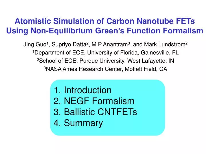
Atomistic Simulation of Carbon Nanotube FETs Using Non-Equilibrium Green’s Function Formalism Jing Guo1, Supriyo Datta2, M P Anantram3, and Mark Lundstrom2 1Department of ECE, University of Florida, Gainesville, FL 2School of ECE, Purdue University, West Lafayette, IN 3NASA Ames Research Center, Moffett Field, CA Introduction NEGF Formalism Ballistic CNTFETs Summary
Introduction: carbon nanotubes McEuen et al., IEEE Trans. Nanotech., 1 , 78, 2002. (see also: R. Saito, G. Dresselhaus, and M.S. Dresselhaus, Physical Properties of Carbon Nanotubes, Imperial College Press, London, 1998.)
Lch ~50nm Gate 8nm HfO2 Pd Pd CNT SiO2 p++ Si Introduction:device performance VG=0.2V nanotube diameter ~1.7 nm -0.1 V -0.4 V -0.7 V -1.0 V -1.3 V tube d ~1.7 nm ( W = 2d ) Javey, Guo, Farmer, Wang, Yenilmez, Gordon. Lundstrom, and Dai, Nano Lett., 2004
Outline Introduction NEGF Formalism Ballistic CNTFETs Summary
Gate [H] S D molecule or device device contacts f1 f2 scattering Nonequilibrium Green’s Function (NEGF) Charge density (ballistic) Current Datta, Electronic Transport in Mesoscopic Systems, Cambridge, 1995
Outline Introduction NEGF Formalism Ballistic CNTFETs Summary
Gate S D atomistic (pZ orbitals ) c t CNTFETs: real-space basis (ballistic) ΣS H= ΣD (m, 0) CNT Recursive algorithm for Gr: O(m3N) Lake et al., JAP, 81, 7845, 1997
Gate n+ n+ i CNTFETs:real-space results 2nd subband interference band gap Confined states
CNTFETs:mode-space approach (ballistic) The qth mode c t (m,0) CNT • S (1,1) and D (N,N) analytically computed • Computational cost: O(N) real space O(m3N) k t
Gate 8nm HfO2 Pd Pd CNT SiO2 p++ Si CNTFETs:mode-space results coaxial G dCNT~1nm i n+ n+ coaxial G 2 modes 2 modes coaxial G VD=0.4V real space real space coaxial G band profile (ON)
CNTFETs:treatment of M/CNT contacts M band discontinuity metallic tube band Kienle et al, ab initio study of contacts in progress
CNTFETs:treatment of M/CNT contacts Gate Metal S metal D tunneling VD=VG=0.4V Charge transfer in unit cell: Leonard et al., APL, 81, 4835, 2002
Gate 8nm HfO2 Pd Pd CNT SiO2 p++ Si CNTFETs:3D Poisson solver Method of moments: Electrostatic kernel: for 2 types of dielectrics available in Jackson, Classical Electrodynamics, 1962 Neophytou, Guo, and Lundstrom, 3D Electrostatics of CNTFETs, IWCE10
CNTFETs:numerical techniques • Non-linear Poisson • Recursive algorithm for • Gaussian quadrature for doing integral • Parallel different bias points • ~20min for full I-V of a 50-nm CNTFET given n: given n: --- --- > > U U scf scf “Poisson” Poisson Iterate Iterate until until self self - - consistent consistent given given U U : : --- --- > n > n scf scf transport equation NEGF Transport
Gate 8nm HfO2 Pd Pd CNT 10 nm SiO2 experiment p++ Si theory CNTFETs:theory vs. experiment VD= -0.3V -0.2V -0.1V Javey, et al., Nano Letters, 4, 1319, 2004 G Bp=0 dCNT ~1.7nm RS=RD~1.7K
Summary A simulator for ballistic CNTFETs is developed - atomistic treatment of the CNT - 3D electrostatics - phenomenological treatment of M/CNT contacts - efficient numerical techniques Theory is calibrated to experiment