Download
1 / 39
430 likes | 634 Vues
Register Transfer & Microoperations. Describing Digital Systems. Digital systems are very complex. They are usually designed and built of different modules that perform specific tasks.

E N D
Describing Digital Systems • Digital systems are very complex. • They are usually designed and built of different modules that perform specific tasks. • The best way to define the operation of these modules is by specifying the registers they contain and the operations possible on the data in these registers.
Example • We can define an adder as a module that: • Interacts with three registers: • Two source registers. • One destination register. • Performs the addition operation on the contents of the source registers and places the result in the destination register.
Microoperations • Operations that specify every modification to the data in the registers are called “microoperations”. • They are simple operations performed on information stored in one or more registers. • Each assembly language instruction can be broken down into multiple microoperations.
Example • The “ADD B” instruction of the 8085 is made up of the following microoperations: • Move the contents of the accumulator to “temporary register” W. • Move the contents of the B register to “temporary register” X. • Add W to X. • Move result of addition back to the accumulator and set the appropriate flags. • Increment the program counter.
Designing a Hardware System • When designing a hardware system, one must specify the following items about the system: • The set of register it contains and their functions. • The set of microoperations that can be performed on the information in these registers. • The sequencing and control of these microoperations. • The microoperations and the control will be translated into the hardware that make up the system.
Register Transfer Language • We can use plain English to specify these registers, operations and their control. • However, the result will be very long and verbose descriptions. • It would be much easier to use symbols to represent (abstract) some of the information. • This abstraction is called a “Register Transfer Language” – RTL. • Register Transfer – operations are performed on data stored in registers and the results are transferred either back to the same registers or to other registers.
Register Transfer Language • Register Transfer Languages are abbreviated, concise representations of the actual description. • They contain ALL the necessary information in shortened descriptions. • They contain ONLY the necessary information. • These languages require that the designer learns a few symbols to represent the different entities and operations in the digital system. • The result is a very powerful tool for expressing hardware design.
Register Transfer Language • The language can be classified into some main statement types • Register Transfer Operations. • Bus and Memory Transfer Operations. • Arithmetic Operations. • Logic Operations. • Shift Operations.
Register Transfer Operations • These are operations that simply denote the transfer of the binary data from one register to another. • First, some definitions: • Special purpose registers are represented using capital letters that specify their function: • PC – Program Counter, AR – Address Register, … • General purpose registers are either represented using an alphabetically ordered list, or an enumerated list. • A, B, C, … • R1, R2, R3, … • Bits in an n-bit register are numbered from 0 (least significant) to n-1 (most significant).
Register Transfer Operations • Register transfers are represented in the following manner: Destination Source • This means, “all of the bits of the source register are copied into the destination register. • For example, R2 R1
Conditions • The previous operation requires that the destination register must have some control which would allow the loading of the register at the required point in time. • This “LOAD” input would only be activated under certain conditions: If (P == 1) { R2 R1 } • This, we write in the following way: P: R2 R1
Hardware Implications • Translating into hardware P: R2 R1 • There has to be two registers called R1 and R2. • R2 must have parallel load capability. • There has to be n wires connecting the output of R1 to the inputs of R2. • There has to be a control signal called P connected to the load input of R2. Control Unit P R2 LD n R1
Bus Transfer Operations • How do we connect all of the registers in the Microprocessor to each other? • Separate connection paths? • Too many wires. • Common bus scheme. • This is the most often used technique to reduce the number of connections needed. • What is a bus? • A bus consists of a set of common wires that are accessed by multiple modules or sub-systems. • And, a mechanism to control who is allowed to use it.
Bus Control • To allow the multiple modules to access the bus without interfering with each other, some mechanism is required to control who uses the bus when. • One common way of controlling access to the bus from several registers is by utilizing a set of multiplexers.
Controlling Access to the Bus Common Wires n n Control Unit S0 n-bit 4 X 1 MUX S1 n n n n R1 R2 R3 R4
Controlling access to the bus • The previous diagram assumes that only the registers will access the bus. • If other modules may use the bus, Tri-state buffers must be used to isolate the bus from the modules not using it. • The tri-state buffers can be added after the outputs of the multiplexers. OR • It is possible to replace the multiplexers with the buffers. However, controlling them would require the same amount of logic as the multiplexers.
Common Wire R0 2 - 4 Decoder 0 Control Unit S0 1 R1 2 S1 3 R2 R3 Controlling Access to the Bus
Bus Transfer Representation • In RTL, busses are usually referred to as BUS1, BUS2, … • A transfer involving the bus can be designated in one of two ways: BUS C, R1 BUS OR R1 BUS C • Even if there is only one bus and all operations utilize it, it is useful to explicitly show the bus in the operations. • It is a common resource that is constantly under contention.
Memory Transfer Operations • A memory read operation has the following stages: • The address is sent to the memory system • The memory system produces the word stored in the specified location • The memory word is read back into the digital system. • In most digital systems: • A special register called the memory address register (MAR) holds the address during the memory operation. • A special register called the memory data register (MDR) holds the data before or after the operation.
Memory Transfer in RTL • In RTL, a memory transfer is represented in a manner similar to a simple register transfer, except that the source or destination is replaced by M[MAR]. Read: DR M[MAR] Write: M[MAR] DR • M[AR] means “the memory location whose address is in the address register AR”.
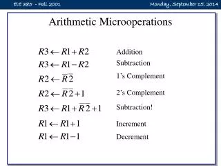
Arithmetic Microoperations • The five main arithmetic microoperations that one encounters when designing any digital systems are: • Addition. • Subtraction. • Increment. • Decrement. • Shift. • Logical Shift. • Arithmetic Shift.
Arithmetic Microoperations • Addition R3 R1 + R2 • Subtraction R3 R1 + R2 + 1 • Increment R2 R2 + 1 • Decrement R2 R2 - 1
Arithmetic Microoperations • What about Multiplication and Division? • Multiplication and Division are either implemented directly in hardware • Then a separate single microoperation is used to specify them. • Or, they may be implemented by repeated addition or repeated subtraction. • Then a sequence of addition, subtraction, and shift microoperations are used to specify them.
Hardware Implications • Binary Adder/Subtractor B3 A3 B2 A2 B1 A1 B0 A0 M FA FA FA FA C4 S3 S2 S1 S0
Hardware Implications • The above circuit can implement all of the following operations
Hardware Implications • What is missing? • Any operation that needs to use the input carry. • Add with Carry • Subtract with Borrow • The input carry is being used to form the 2’s complement. • If the above operations are needed, a completely different circuit must be used.
3 3 3 3 2 2 2 2 1 1 1 1 S0 S0 S0 S0 0 0 0 0 S1 S1 S1 S1 4X1 MUX 4X1 MUX 4X1 MUX 4X1 MUX Y Y Y Y Y Y Y Y X X X X C C C C FA FA FA FA C C C C S S S S Hardware Implications – Arithmetic Circuit 0 B3 A3 B2 A2 B1 A1 B0 S0 S1 A0 Cin D0 D1 D2 D3 Cout
Logic Microoperations • Logic microoperations specify binary operations for strings of bits stored in registers. • These operations treat the values in the registers simply as a string of unrelated bits. • These operations process the data in the registers bit-wise. i.e. bit by bit.
Logic Microoperations • There are many possible logic operations. • However, the following are the most common (and useful). • Clear (set to 0) F 0 • AND F A B • OR F A B • XOR F A B • NOT F A • Set (set to 1) F 1
Hardware Implications • Logic circuit (per bit). Ai Bi S0 3 2 1 0 Control Unit 4 X 1 MUX S1 Ei
Hardware Implications • The above circuit can implement all of the mentioned operations.
Shift Microoperations • Shift microoperations are mainly used for serial transfer of data. • They are also used in conjunction with arithmetic, logic and other operations. • The contents of a register can be shifted to the left or to the right. • At the same time, the first bit (from the right or the left) receives its input from the serial input. • In all shift operations, the source and destination registers must be the same.
Types of Shift Operations • Logical shift. • A shift where the serial inputis set to 0. • shl and shr. R1 shl R1 R1 shr R1 • Circular shift (rotate). • A shift where the serial input is set to the last bit. • cil and cir. R1 cil R2 R1 cir R2
Types of Shift Operations • Arithmetic shift right: • Shifting to the right divides the number by 2. • The serial input is set to the sign bit to preserve the sign of the number. • ashr. R1 ashr R1 Rn-1 Rn-2 R2 R1 R0
Types of Shift Operations • Arithmetic shift left: • Shifting to the left multiplies the number by 2. • The serial input is set to 0. • The sign bit (Rn-1) is replaced by bit Rn-2. • If Rn-2 is not equal to Rn-1, shift overflow occurs. • ashl. R1 ashl R1 0 Rn-1 Rn-2 R2 R1 R0
Hardware Implications A3 A2 A1 A0 A3 0 0 A0 0 A3 cil cir shl shr ashl ashr 0 Shift Right 1 Shift Left 1 0 s 1 0 s 1 0 s 1 0 s 2X1 MUX 2X1 MUX 2X1 MUX 2X1 MUX H3 H2 H1 H0 A – Register Output H – register Input
Arithmetic Logic Shift Circuit - ALU • Taking all of the above together, we can design a “composite” circuit that implements all of the arithmetic, logic and shift operations. • To facilitate this and not introduce too much connection complexity, most computer designs employ “temporary” registers. • The information is transferred to these registers before an ALU operation. • The ALU operates on the contents of these registers. • The results of the ALU operation are stored in the destination register directly.