Download
1 / 17
180 likes | 264 Vues
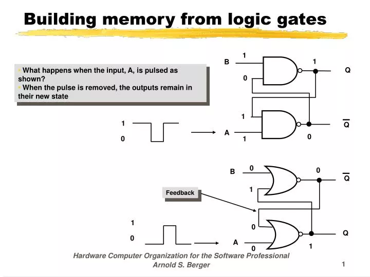
Building memory from logic gates. 1. 1. B. Q. What happens when the input, A, is pulsed as shown? When the pulse is removed, the outputs remain in their new state. 0. 1. 1. Q. A. 0. 0. 1. 0. 0. B. Q. 1. Feedback. 1. 0. Q. 0. A. 1. 0. Type “D” Flip-Flop. S. D. Q.

E N D
Building memory from logic gates 1 1 B Q • What happens when the input, A, is pulsed as shown? • When the pulse is removed, the outputs remain in their new state 0 1 1 Q A 0 0 1 0 0 B Q 1 Feedback 1 0 Q 0 A 1 0 Hardware Computer Organization for the Software Professional Arnold S. Berger
Type “D” Flip-Flop S D Q CLK Q R • Design to change its output state synchronously with a clock signal input • State of signal on the D input (data) is transferred to the Q output on the rising edge of the clock • Set/Reset inputs are asynchronous SET=0 ( Q > 1 ) S R D CLK Q Q t0 t1 t2 t3 t4 t5 t6 t7 t8 t9 t10 t11 Timing Diagram RESET=0 ( Q > 0) Hardware Computer Organization for the Software Professional Arnold S. Berger
Inside the “D” Flip-flop Try this out on your Digital Simulator. It works! Hardware Computer Organization for the Software Professional Arnold S. Berger
The ‘D’ flip-flop divides by two S D Q CLK Q R 1 Rising edges CLK D Q /Q • The /Q output is fed back to the D input • Ignoring propagation delay, the Q output • after the rising edge of the clock agrees • with the D input before the rising edge of • the clock. • The waveform at the Q output has twice the • period (half the frequency) of the waveform • at the clock input. 1 Hardware Computer Organization for the Software Professional Arnold S. Berger
Cascading D-FFs clock Hardware Computer Organization for the Software Professional Arnold S. Berger
The “D” FF as a counting element Q0 S S S S D D D D Q Q Q Q CLK Q CLK CLK CLK Q Q Q R R R R • A 16-bit binary ripple counter • Given the name because the pulses “ripple” through the circuit Q1 Q2 Q3 1 Clock in RESET • Each “D” FF divides the incoming clock frequency by 2X • RESET sets all Q output to 0 without a clock signal (asynchronous) • Counts as fast as the first stage can toggle, but cannot be read until the count has rippled through to the last stage • Can build counter/dividers of any length, any binary divisor • Clock frequency at output Q3 equals fClock in ÷ 16 Hardware Computer Organization for the Software Professional Arnold S. Berger
Waveform of a 16-bit counter Hardware Computer Organization for the Software Professional Arnold S. Berger
“D” FF as a shift register Q2 Q1 S S Q Q D D CLK CLK Q Q Q Q R R Q0 Q3 1 S S Shift data in Shift data out Q Q D D CLK CLK R R RESET Clock in • Shift register moves data through successive stages on each clock pulse • Used for serial data communications, multiplication ( why ?), image processing • Basis for UART ( Universal Asynchronous Receiver/Transmitter ) • Data can be read in serially and then read out in parallel • Serial data communications limits the number of signal wires needed to transmit bytewide • data ( Example shown here is a nibble ) Hardware Computer Organization for the Software Professional Arnold S. Berger
Serial data transmission • The data value is synchronized with the rising edge of the clock. • One rising edge (clock pulse) is required for each data bit being transmitted • In this example the data is transmitted most significant bit to least significant bit most significant bit 0 1 1 0 least significant bit DATA CLOCK Hardware Computer Organization for the Software Professional Arnold S. Berger
Waveform for the shift register D Q0 Q1 Q2 Q3 CLK 0 1 1 0 t1 t2 t3 t4 Hardware Computer Organization for the Software Professional Arnold S. Berger
“D” flip-flop as a storage register Q Q Q Q Q Q Q Q D D D D D D D D D0 D1 D2 D3 D4 D5 D6 D7 D0 D1 D2 D3 D4 D5 D6 D7 D0 Q0 D1 Q1 D2 Q2 D3 Q3 D4 Q4 D5 Q5 D6 Q6 D7 Q7 Clock in INPUT DATA OUTPUT DATA Hardware Computer Organization for the Software Professional Arnold S. Berger
An 8-bit storage register D0 D1 D2 D3 D4 D5 D6 D7 D0 D1 D2 D3 D4 D5 D6 D7 D0 Q0 D1 Q1 D2 Q2 D3 Q3 8-bit Storage Register D4 Q4 D5 Q5 D6 Q6 D7 Q7 Clock in INPUT DATA OUTPUT DATA Hardware Computer Organization for the Software Professional Arnold S. Berger
State representation of a ‘D’ FF • Can best represent the design of state machines with a table or a graphical description ( ignore the asynchronous set/reset inputs) • Assume the transitions occur on the rising edge of clk Current Current Next Input State State D Q Qn D Q CLK Q 0 0 0 State 1 1 1 0 0 1 1 01 10 0 1 1 0 0 1 input Hardware Computer Organization for the Software Professional Arnold S. Berger
State machine for a 4-bit counter 0100 0011 0010 0001 0000 • No matter what state you start from, the next state is always determined • If RESET were made synchronous, we would add an arrow from every state back to 0000. 0101 1111 0110 1110 0111 1101 1000 1001 1010 1011 1100 Hardware Computer Organization for the Software Professional Arnold S. Berger
4-bit memory array 16 by 4 memory array Memory Cell Address 0 0 0 0 1 0 0 0 0 1 0 0 1 1 0 0 0 0 1 0 1 0 1 0 0 1 1 0 1 1 1 0 0 0 0 1 1 0 0 1 0 1 0 1 1 1 0 1 0 0 1 1 1 0 1 1 0 1 1 1 1 1 1 1 Memory cell data ADDRESS IN DATA OUT Ain Bin Cin Din Aout Bout Cout Dout Hardware Computer Organization for the Software Professional Arnold S. Berger
State Machine The output values in the register is the address of the memory cell for the data that determines the next state of the outputs after the clock arrives Q0 Q0 D0 A0 D0 Q1 Q1 D1 A1 D1 Q2 Q2 D2 A2 D2 Q3 Q3 D3 A3 D3 16 x 4 Memory Array CLK REGISTER Hardware Computer Organization for the Software Professional Arnold S. Berger
Why do we need the D flip-flop? Case A A B C Case B B D A Q C D FF clk Clock input Hardware Computer Organization for the Software Professional Arnold S. Berger