Download
1 / 33
340 likes | 357 Vues
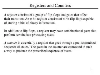
Registers and Counters. Registers. Register is very important building blocks. A data register is often used to store binary information. A register might be used to accept input data from an alphanumeric keyboard and the present this data to the circuitry used to display on the CRT screen.

E N D
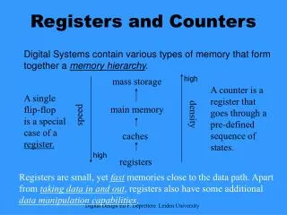
Registers • Register is very important building blocks. • A data register is often used to store binary information. • A register might be used to accept input data from an alphanumeric keyboard and the present this data to the circuitry used to display on the CRT screen. • Register is a group of flip flops that can be used to store a binary number. • n-bit register has n flip flops and each FF stores one bit. • Two basic functions: data storage and data movement. • A binary register also performs very important arithmetic operations such as complementation, multiplication, and division.
D0 D Q Q0 C clk D0 Q0 D1 D Q Q1 Q1 D1 C D2 Q2 D Q Q2 D2 C D3 Q3 clk D3 D Q Q3 C Four bit Register Symbol Circuit
Shift Registers • A shift register can also be connected to form a number of different types of counters (count the clock pulses). • The FF must be connected such that the binary number can be entered (shifted in) into the register and possibly shifted out. • A group of flip flops connected to provide either shifted in or shifted out or both of these functions is called a shift register. • In the shift register, binary number can be moved from one place to another in either of two ways: • Shifting the data 1 bit at a time in a serial fashion either from LSB or MSB. This technique is referred to as serial shifting. • Shifting all the data bits simultaneously which is referred to as parallel shifting.
Shift Registers • Shift registers are a type of sequential logic circuit, mainly for storage of digital data. • They are a group of flip-flops connected in a chain so that the output from one flip-flop becomes the input of the next flip-flop. • All the flip-flops are driven by a common clock, and all are set or reset simultaneously. • A shift register is a digital memory circuit found in calculators, computers, and data-processing system.
Types of Registers • There are two ways to shift the data into a register (serial or parallel) and similarly two ways to shift the data out of a register. • This lead to construction of four basic types of registers: (d) Parallel in- Parallel out
1. Shift Registers – Serial-in Serial-out • Consider 4 D flip flops connected and forming 4-bit shift register. • A common clock provides trigger at its negative edge to all the FFs. This negative transition of the clock NT is referred to as a shift pulse. • As output of one D FF is connected to the input of next at every clock trigger and data stored in one FF is transferred to the next. • For this circuitry, transfer takes place like this Q to R, R to S, S to T and the serial data input is transferred to Q.
Shift Registers – Serial-in Serial-out • A basic four-bit shift register can be constructed using four D flip-flops. • The operation of the circuit is as follows. • The register is first cleared, forcing all four outputs to zero. • The input data is then applied sequentially to the D input of the first flip-flop on the left (FF0). During each clock pulse, one bit is transmitted from left to right. • Assume a data word to be 1001. The least significant bit of the data has to be shifted through the register from FF0 to FF3. • In order to get the data out of the register, they must be shifted out serially.
Shift Registers – Serial-in Serial-out A DQRS=0000; QRST=0000 B DQRS=0000; QRST=0000 C DQRS=1000; QRST=1000 D DQRS=0100; QRST=0100
Shift Registers – Serial-in Serial-out • Points to note: • At every clock pulse, the first flip flop is loaded with the value of the data in stream • The data that was in this flip flop is then loaded into the second and so on. • The data can be taken out of the last flip flop in serial form or it can be taken from all outputs at the same time – parallel form.
Qa Qb Qc Qd Da D Q D Q D Q D Q C C C C A B C D Shift Registers – Serial-in Serial-out • For each flip flop there is a delay between clock pulse and output. This delay provides time for the next flip flop in the chain to load the data from the previous stage. data clock Qa Qb etc
2. Shift Registers – Serial-in Parallel-out • In the second type of shift registers, data is shifted serially, but shifted out in parallel. • In order to shift the data out in parallel, it is simply necessary to have all the data bits available as outputs at the same time. • This is accomplished by connecting the output of each FF to output pin. • For eg. an 8-bit shift register would have eight output lines-one for each FF in the register.
2. Shift Registers – Serial-in Parallel-out • This configuration allows conversion from serial to parallel format. • Data is input serially, as described in the SISO section above. • Once the data has been clocked in, it may be either read off at each output simultaneously, or it can be shifted out. • If four data bits are shifted in by four clock pulses via a single wire at Input data, the data becomes available simultaneously on the four Outputs Q0 to Q3 after the fourth clock pulse • In this configuration, each flip-flop is edge triggered. Four-bit binary number 1001 is shifted to the Q outputs of the register
2. Shift Registers – Serial-in Parallel-out • The Shift register 74LS91 is exactly similar to 54/74164 8-bit register with 2 exceptions: • Each FF is available as an output – all 8 bits of any number stored in the register are available simultaneously as an output (parallel data output). • Each FF has an asynchronous clear input. Thus it is applied through amplifier and will reset (clear) every FF. • Since It is an asynchronous signal, it can be applied at any time without regard to the clock waveform and this signal is level sensitive.
2. Shift Registers – Serial-in Parallel-out • Let’s take a look at the gated serial inputs A and B. Suppose that the serial data is connected to A; then B can be used as a control line. • B is held high: The NAND gate is enabled and the serial input data passes through the NAND gate inverted. The input data is shifted serially into the register. • B is held low: The NAND gate output is forced high, the input data stream is inhibited, and the next positive clock transition will shift a 0 into the first flip flop. Each succeeding positive clock transition will shift another 0 into the register. After eight clock pulses, the register will be full of zeros.
2. Shift Registers – Serial-in Parallel-out • This fig. shown the response of a 54/74164. The serial data is input at A (pin 1), while a gating control signal is applied at B (pin 2). The first pulse occurs at time A and simply resets all FF to 0. • The clock begins at time B, but the first PT does nothing since the control line is low. At time C, the control line goes high and the first data bit (a 0) is shifted into the register at time D. • The next 7 data bits are shifted in, in order, at times E, F, G, H, I J and K.
The clock remains high after time K, and the 8-bit number 0010 1100 now resides in the register and is available on the eight output lines. • This assumes that the LSB was shifted in the first and appears at QH. • Notice that the clock must be stopped after its PT at time K, otherwise shifting will continue and the data bits will be lost. • Finally, another clear pulse occurs at time L, the FFs are all reset to 0, and another shift sequence may begin. • Incidentally, the register can be cleared by holding the control line at B low and allowing the clock to run for eight PTs. This simply shifts eight 0s into the register
3. Shift Registers – Parallel-in Serial-out • The third types uses parallel entry of data into register. • There are a number different techniques for the parallel entry of data, but focused on commercially available TTL. • Eg.: 54/74166 which is an 8-bit shift register and the same circuit is repeated eight times. • TTL (Transistor–transistor logic)
3. Shift Registers – Parallel-in Serial-out • According to TTL functional description data sheet, 54/74166 is an 8-bit shift register, capable of either serial or parallel data entry, and serial data output. • Notice that there are 8 RS FFs, each with some attached logic circuitry. • Recall the concepts of RS FF and the attached inverter that forms a D FF • If a data bit X is to be clocked into the FF, the complement of X must be present at the input. • For instance, if X = 0, then R = 0 and S = 1 and a 1 will be clocked into the FF when the clock transitions.
3. Shift Registers – Parallel-in Serial-out • Now add a NOR gate. • If one leg of this NOR gate is at ground level, a data bit X at the other leg, which is simply inverted by the NOR gate. • If X = 1, then at the output of the NOR gate X = 0, allowing a 1 to be clocked into the FF. • This NOR gate offers the option of entering data from two different sources, either X1 or X2. • Holding X2 at ground will allow the data at X1 to be shifted into the FF. • Conversely, holding X1 at ground will allow data at X2 to be shifted in.
3. Shift Registers – Parallel-in Serial-out • Next, addition of two AND gates and two inverters that will allow the selection of data X1 or data X2. • If the control line is high, the upper AND gate is enabled and the lower AND gate is disabled. • Thus X1 will appear at the upper leg of the NOR gate while the lower leg of the NOR gate will be at ground level. • On the other hand, if the control line is low, the upper AND gate is disabled while the lower AND gate is at ground level. • Control is high: Data bit at X1 will be shifted into the FF at the next clock transition. • Control is low: Data bit at X2 will be shifted into the FF at the next clock transition.
3. Shift Registers: Parallel-in Serial-out54/74166 8 bit Shift Register
Parallel data inputs D0 D1 D2 D3 D D D D Q Q Q Q CLK C C C C Q0 Q1 Q2 Q3 Parallel data outputs 4. Shift Registers – Parallel-in Parallel-out • The fourth type of register is designed such that data can be shifted either into or out of the register in parallel.
4. Shift Registers – Parallel-in Parallel-out • 74ALS174 is an 6 bit register that has parallel inputs D5 through D0 and parallel-outputs Q5 through Q0. • It is simply a parallel arrangement of six D-FF. • Each FF is negative-edge triggered and thus a PT will shift data into the register. • The six data bits, D1 through D6 are all shifted into the register in parallel. • The stored data is immediately available, in parallel, at the outputs Q1 through Q6.
4. Shift Registers – Parallel-in Parallel-out • Another example is 54/74198 is an 8-bit TTL having both parallel input and parallel output capacity. • It uses positive edge-triggered FFs. • Notice that a 24-pin package is required since 16 pins are needed just for the input and output data lines. • It is also used to shift data through the register in either direction – shift left and shift right.
4. Shift Registers – Parallel-in Parallel-out • Since this register is used to store the data, it is referred to as data register or data latch. • Notice that it is not possible to shift stored data either to the right or to the left. • A low level at the clear input will immediately reset all FFs low. • The clear input is asynchronous – it can be done at any time and it takes precedence over all other inputs.
4. Shift Registers – Parallel-in Parallel-out • Another example is 54/7495A is a 4-bit parallel access shift register. • It can be packaged in a 16-pin DIP. • It has serial data input and can be used to shift data to the right (from QA toward QB) and to the left.
Registers/Shift registers • Summary • Registers consist of a group of D-type latches or flip-flops which are clocked simultaneously to store a binary word • set-up and hold times must be observed • Shift registers allow data to be moved from one bit position to another • used for parallel«serial conversion and some types of arithmetic operations