Download
1 / 25
250 likes | 438 Vues
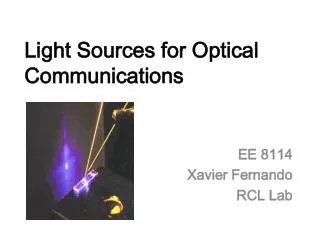
2 光源 (Optical Sources) 與檢光器 (Photodetectors) 重要參數量測. LED’s and lasers are important optical sources for the electro-optical transformation in fiber optic communications. They are essential for optical transmitters .

E N D
2 光源(Optical Sources)與檢光器(Photodetectors)重要參數量測 • LED’s and lasers are important optical sources for the electro-optical transformation in fiber optic communications. They are essential for optical transmitters. • PIN photodiodes and APD are important optical detectors for the opto-electronic transformation in fiber optic communications. They are essential for optical receivers.
LED sources are low cost. LED sources can be used for short-distance fiber-optic systems. Type LED’s are: 2.1.1 Surface-Emitting LED (SLED) 2.1.2 Edge-Emitting LED (EELED) 2.1 Light Emitting Diodes
2.1.1 Surface-Emitting LED • A SLED can be a hetero-junction diode. It can be made by low band gap materials sandwiched between high band gap materials. • There are no mirrors to provide optical resonance. • A SLED can be used as a multimode source.
2.1.1 Surface-Emitting LED • The electrons and holes recombine and lose energy spontaneously by emitting photons in all directions • In the SLED, light wave comes out of the diode from the surface as shown in the figure. Active Layer Spontaneous Emission Photons Spontaneous Emission Photons Fig 2.1. Side view of a surface-emitting LED
2.1.2 Edge-Emitting LED • The EELED can be composed of two sections: a gain section and an absorption section. • The gain section is forward biased to provide an optical gain. • The absorbersection is reverse biased to provide an optical absorption. : AR(Antireflection) Coating : Optical gain : Optical absorption Fig 2.2. Side-view of an edge-emitting LED (EELED)
2.1.2 Edge-Emitting LED • The absorption section prevents the optical amplifier from lasing. • The output of the gain section is antireflection-coated. • The gain section can be a semiconductor optical amplifier(SOA). It produces amplified spontaneous emission (ASE).
2.2 Lasers • Laser means “Light Amplification by Stimulated Emission of Radiation.” • A laser produces coherent light by stimulated emission. It can be used in optical transmitters for telecommunications and data communications. • Type of lasers: • 2.2.1 Fabry-Perot laser (FP laser) • 2.2.2 Distributed Feedback laser (DFB laser) • 2.2.3 Vertical Cavity Surface-Emitting laser • (VCSEL laser)
2.2.1 Fabry-Perot Lasers • The Fabry-Perot laser is composed of semiconductor amplifier and reflective mirrors. • It is low cost. • It has substantial spectral width and can be used with low chromatic-dispersion fibers. Mirror Mirror : Current Input & Output Layer : Gain Region & Optical Waveguide Fig 2.3 Cross-section of a Fabry-Perot laser diode
2.2.1 Fabry-Perot Lasers • The optical amplifier gain increases as the current increases. • Lasing occurs if the amplifier gain is equal to or large than the mirror loss. • The threshold current, slope efficiency, and spectral width are basic parameters. Fig 2.4 Light vs. Current characteristic
2.2.1 Fabry-Perot Lasers • The gain, the mirror loss, and the location of longitudinal modes of the laser are shown in the Fig 5 as functions of wavelength. • The spacing between the possible lasing wavelengths (mode spacing) is determined by the distance between the two mirrors. Fig 2.5 The gain, mirror loss,and longitudinal mode location.
2.2.2 Distributed Feedback Lasers(DFBs) • The DFB laser is similar to an FP laser with the addition of a Bragg reflector structure located near the light-emitting region. Metal Layer Bragg Reflector Output Active Layer Metal Layer Fig 2.6 Cross-section of a DFB laser
2.2.2 Distributed Feedback Lasers(DFBs) • The Bragg grating can be made by introducing a periodic change in the index of the refraction in the waveguide. • Each period of the grating reflects a small amount of light back in the opposite direction. • The Bragg grating has a high reflectivity at the wavelength where the grating period is one-half of the wavelength of light in the semiconductor material. It can be used as a mirror.
2.2.2 Distributed Feedback Lasers(DFBs) Mirror Loss(dB) • The reflection pass band in a typical Bragg grating is only a few nanometer wide. • This frequency-dependent reflectivity makes the laser power to emit in a single longitudinal mode Amplifier Gain (dB) Fig 2.7 Bragg grating reflectivity, amplifier gain,and longitudinal mode location.
2.2.3 Vertical Cavity Surface-Emitting Laser(VCSEL) Bragg Mirror • Vertical cavity lasers emit perpendicular to the top plane of semiconductor wafer as shown in Fig 8. • The VCSEL uses a multilayer dielectric Bragg mirror that is grown directly on the semiconductor surface. 10 Isolation Active Layer Bragg Mirror Substrate Fig 2.8 Cross-section view of a VCSEL
2.2.3 Vertical Cavity Surface-Emitting Laser(VCSEL) • The length of optical amplifier in this VCSEL is short (on the order of 100 nm). • This short amplifier length limits the available gain from the amplifier to a small value. Amplifier Gain (dB) Mirror Loss(dB) Fig 2.9 Mirror loss,amplifier gain,and longitudinal mode location
2.2.3 Vertical Cavity Surface-Emitting Laser(VCSEL) • A wider spectral width is often designed into VCSEL to avoid mode-selective loss in multimode fiber applications. • The VCSEL is low cost. • The VCSEL has higher output power and higher modulation rates than surface-emitting LED.
2.3Source Measurements [from “Fiber Optic Test and Measurement”, edited by D. Derickson]
2.3 Source Measurements • Using the OSA, we can obtain the optical spectrum of an optical source such as a LED or a laser. • The threshold current and slope efficiency of lasers can be obtained from the curve of power vs. pumping current, which can be measured by a power meter. • Linewidth and chirp measurement will be discussed latter OSA Optical Source
2.4 p-i-n Photodiodes • The optical receiver detects the lightwave signal and then conditions the resulting electrical signal to the appropriate levels. • Photodiodes are used for optical to electrical conversion.
2.4 p-i-n Photodiodes • The hetero-junction p-i-n diodes consists mainly of three layers of semiconductors with different band gaps and different doping concentrations. • A low-bandgap material is usually used as the i (intrinsic) layer that absorbs incoming photons. I P in out Electrical Contact Light Absorption Layer P (InP) i (InGaAs) n (InP) n substrate Fig 2.10 p-i-n photodetector diagram
2.4 p-i-n Photodiodes • The p-i-n photodiode can have a high electric field across the intrinsic layer. • Electron and hole pairs are created in the layer if photons are absorbed. • The electric field sweeps these carriers out to an external electrical circuit. • An InGaAs undoped layer surrounded by doped p and n InP material can be used to make a p-i-n photodiodes.
2.5 APD Detectors • A diagram of an avalanche photodector(APD) is shown in Fig 11. • It can improve the sensitivity compared to a p-i-n photodiode. • The APD provides low-noise, high-bandwidth, and photo-current gain. Electrical Contact I P in out Light Absorption Layer n (InGaAs) Multiplication Layer n (InP) p+ (InP) p+ substrate Fig 2.11 APD diagram with separate absorption and multiplication regions.
The APD use a low-bandgap semiconductor absorption region. The photo-generated electrons are accelerated to high velocities and lead to avalanche process. The high energy electrons collide with the lattice to generate new free carriers in avalanche processes. The ideal low-noise APD multiplies the number of electrons but does not multiply holes in the avalanche process. The APD require a high-bias voltage to produce avalanche conditions. The avalanche process is also temperature-dependent. 2.5 APD Detectors
2.6 Detector Measurements • The detector response can be measured by using light sources of different wavelengths and an ammeter. input optical power • Responsivity R=current (I0) / input optical power(Pi) I P ( ) λ 0 OUT A i
2.6 Detector Measurements • The dark current Idark is the current that flows through the detector in the absence of light. • The shot noise is given by 2e( Idark + Isignal). • The noise equivalent power (NEP) is the amount of light at a given wavelength that is equivalent to the noise level of the detector.The noise can be obtained from the spectrum measured by an electrical spectrum analyzer. • The time domain response can be obtained if the ammeter is replaced by an oscilloscope.