Download
1 / 47
500 likes | 645 Vues
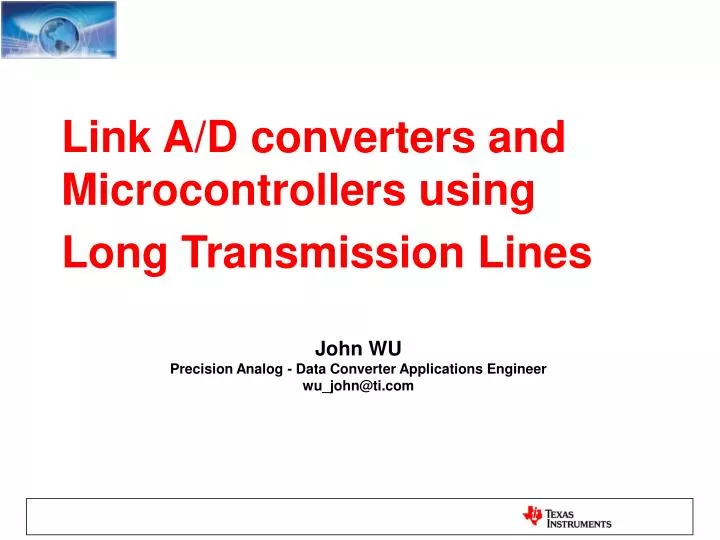
Link A/D converters and Microcontrollers using Long Transmission Lines. John WU Precision Analog - Data Converter Applications Engineer wu_john@ti.com. Transmission Line Effect Considerations. Definition of the Highest Frequency Signal Transmission Line Model Reflection Concept

E N D
Link A/D converters and Microcontrollers using Long Transmission Lines John WUPrecision Analog - Data Converter Applications Engineerwu_john@ti.com
Transmission Line Effect Considerations • Definition of the Highest Frequency Signal • Transmission Line Model • Reflection Concept • Termination Topology • Crosstalk Analysis
Definition of the highest frequency signal What is the highest frequency signal in a 2.25MHz sample clock rate ADC ?
Definition of the highest frequency signal The highest frequency signal is determined by the signal rise or fall time
Rise Time vs. Bandwidth The rise time and bandwidth are related by: For example: clock rate = 2.25 MHz, trise CLK = 10 ns trise Data= 2 ns The highest frequency signal or bandwidth is: = 175MHz
Rise Time Measurement • The displayed Tr = 2ns (10-90%) on an oscilloscope • 3-dB bandwidth of a probe is 500MHz (Tr = 0.7ns) • 3-dB bandwidth of an oscilloscope input is 350MHz (Tr=1ns) • What is the measured input signal Tr ?
Rise Time Degradation • Tdisplayed2= Tprobe2 + Tscope2 + Tsignal2 • Tsignal2 = Tdisplayed2 -Tprobe2 -Tscope2 • Tsignal = SQRT(22 - 0.72 - 12 )=1.6ns! • 1.6ns) = 220MHz
Critical Microstrip Length What is the critical length of a microstrip that must be considered as transmission line?
Critical Microstrip Length • Tr x 15% = 1.6ns x 15% = 226 ps • = 1.5 inch
Г Reflection Factor Zo Z L If Z L >> Zo; Г = +1 If Z L<< Zo; Г = -1
Critical Length of a Transmission Line What is the critical length of a transmission line that must be terminated?
Source Termination Trace & Cable Terminations Driver Receiver Zo = 50 W Rt Rs Rt + Rs = Zo
Trace & Cable Terminations • AC termination AC Termination
Daisy Chain Routing with Stubs Place of Terminations Clock Source Clock Bus Termination Resistor Stub Device 1 Device 2 Device Pin BGA Ball
Short stubs create signal integrity problems Stub Length=0.5” Stub Length=0.25” Reference: Altera application note 224
Daisy Chain Routing without Stubs Device Pin BGA Ball Clock Source Clock Bus Device 1 Device 2 Termination Resistor
Star Routing Clock Bus Device 1 Termination Resistor Device 2 Clock Source Device 3 Device Pin BGA Ball
Parallel Fly-By Termination Vcc R1 Zo = 50 W Receiver Device (BGA Package) R2
Differential Pair (LVDS) Fly-By Termination Receiver Device (BGA Package) Zo=50 W 100 W Zo=50 W
Crosstalk Analysis • Cross Talk occurs on PCB and twisted wire cable
Magnetic & Electric Fields of Parallel Transmission Line Aggressor Trace Victim Trace Aggressor Trace Victim Trace Magnetic Field Electric Field Ground Plane Ground Plane
FEXT Measurement Inductive or Capacitive Coupling ?
Conclusions • The highest frequency signal is determined by switching time • Transmission line model must be used when propagation delay time is greater than 15% of Tr • Termination technique dramatically reduces reflection and crosstalk Q&A
Acknowledgement Thanks Phil Lizzi for providing the “real life” transmission line application example Reference: • “Managing Signal Quality”Mentor Graphics/Xilinx, 2005http://www.xilinx.com/publications/xcellonline/xcell_53/xc_pdf/xc_mentor53.pdf • “High-Speed Board Layout Guideline” Altera application note 224, Sept. 2003