Download
1 / 30
320 likes | 507 Vues
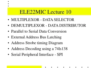
ELE22MIC Lecture 10. MULTIPLEXOR - DATA SELECTOR DEMULTIPLEXOR - DATA DISTRIBUTOR External Address Bus Latching Address Strobe timing Diagram Address Decoding using a 74LS138. Multiplexor - Data Selector. Multiplex (MUX) many inputs to one output

E N D
ELE22MIC Lecture 10 • MULTIPLEXOR - DATA SELECTOR • DEMULTIPLEXOR - DATA DISTRIBUTOR • External Address Bus Latching • Address Strobe timing Diagram • Address Decoding using a 74LS138
Multiplexor - Data Selector • Multiplex (MUX) many inputs to one output • Switch selects the one signal source from many input signals. • Like Stereo HiFi source selection switch
Two Input Multiplexor Output = (Input0 & Select#) | (Input1 & Select)
74F151 8-Input MUX Pin Names and Loading / Fanout
External Address Latch • The Address Bus and Data Bus are multiplexed, and output to the 68HC11’s Port C pins. So that we can utilise external RAM, ROM & Peripherals (in expanded mode MODA/B) • The M.A.R. is presented on A0..A7/D0..D7 pins • The AS pin goes high to load the low 8 bits of the address into the external address latch. • An external address latch extends the internal memory address to create a system’s external address bus.
Applications of a de-multiplexor • The Memory Chip Select device used on the original IBM PC is a 74LS138 de-multiplexor. • The 74LS138 is used to activate 1 of 8 lines based on the conditions of the three binary select inputs A, B & C, and the three enable inputs. • The 74LS138 Outputs are “Active Low”.
74LS138 8-Output DEMUX De-Multiplex one input to many outputs -Reverse operation of a multiplexor 74LS138 Truth Table
DeMultiplexor • The 74LS138 can be implemented by the logic shown. • The 54LS138 is identical in function, but can operate over the “Mil-spec” -55°C to 125°C Temperature Range. • The 74LS138 can operate over the Commercial 0°C - 70°C Temperature Range.
Address Decoding & Chip Select • A15 -> G1#, E -> G, A14 -> A2, A13 -> A1 • R/W# -> A0 • Chip is enabled when A15 = 0 & E is High • Y2 = (A14#) & (A13) & Write (R/W#=0) & E • Y3 = (A14#) & (A13) & Read (R/W#=1) & E • Y4 = (A14) & (A13#) & Write (R/W#=0) & E • Y5 = (A14) & (A13#) & Read (R/W#=1) & E
68HC11 Flash Technology (2) Erasure of Cells is performed by providing a tunnelling voltage to the control gate which causes the charge on the floating gate to be removed. When read, each cell returns a logical ‘1’ value.
68HC11 Flash Technology (3) Programming of Cells is performed by providing a tunnelling voltage to the control gate which causes the charge to be placed on the floating gate. The write process writes the ‘0’s into each cell.
Bus Design Rules Bus lines have very low line impedances (20 .. 40 Ohms). • Bus lines have to be terminated to prevent line reflections (signal distortion, circuit malfunctions due to undershoots). • Take care of propagation times (25 ns/m). Settling time of signals on TTL-type buses is 2 x tp (no incident wave switching). • Take care of control lines (clock, read, write, etc.). • Provide shielding between control lines and data / address lines.
Bus Design Rules • A multiplexed data and address bus reduces design problems (50% less signal lines and 50% less line drivers). • Driver output current is 100 mA/line. Provide adequate and low inductance GND return path (simultaneous switching)! • Rule of thumb: 25% of all backplane connector pins have to be GND lines! • Use multilayer boards with separate GND and Vcc plane for backplanes.
Acknowledgements • I used Altium Protel 98 and Protel DXP to create these schematic diagrams • Logic Timing Diagrams are from Texas Instruments (TI) Logic Selection Guide - Digital Design Seminar • National Semiconductor data sheets 74LS138. • Motorola 11rm.pdf Reference Manual