Download
1 / 73
1.08k likes | 1.8k Vues
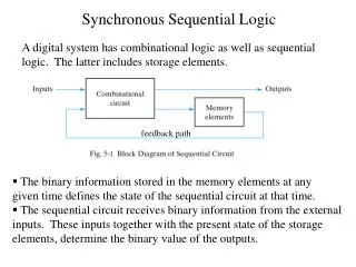
Chapter 5 Synchronous Sequential Logic 5-1 Sequential Circuits. Every digital system is likely to have combinational circuits, most systems encountered in practice also include storage elements , which require that the system be described in term of sequential logic .

E N D
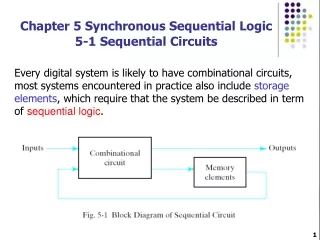
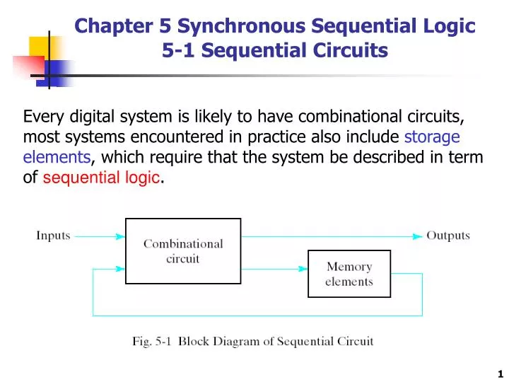
Chapter 5 Synchronous Sequential Logic5-1 Sequential Circuits Every digital system is likely to have combinational circuits, most systems encountered in practice also include storage elements, which require that the system be described in term of sequential logic.
Synchronous Clocked Sequential Circuit A sequential circuit may use many flip-flops to store as many bits as necessary. The outputs can come either from the combinational circuit or from the flip-flops or both.
5-2 Latches SR Latch The SR latch is a circuit with two cross-coupled NOR gates or two cross-coupled NAND gates. It has two inputs labeled S for set and R for reset.
SR Latch with Control Input The operation of the basic SR latch can be modified by providing an additional control input that determines when the state of the latch can be changed. In Fig. 5-5, it consists of the basic SR latch and two additional NAND gates.
D Latch One way to eliminate the undesirable condition of the indeterminate state in SR latch is to ensure that inputs S and R are never equal to 1 at the same time in Fig 5-5. This is done in the D latch.
Graphic Symbols for latches A latch is designated by a rectangular block with inputs on the left and outputs on the right. One output designates the normal output, and the other designates the complement output.
5-3 Flip-Flops The state of a latch or flip-flop is switched by a change in the control input. This momentary change is called a triggerand the transition it cause is said to trigger the flip-flop. The D latch with pulses in its control input is essentially a flip-flop that is triggered every time the pulse goes to the logic 1level. As long as the pulse input remains in the level, any changes in the data input will change the output and the state of the latch.
Clock Response in Latch In Fig (a) a positive level response in the control input allows changes, in the output when the D input changes while the clock pulse stays at logic 1.
Edge-Triggered D Flip-Flop The first latch is called the master and the second the slave. The circuit samples the D input and changes its output Q only at the negative-edge of the controlling clock. D 1 1 0 0 1 1 … Y 1 1 0 0 1 1 … Q ? 1 1 0 0 1 …. CLK
D-Type Positive-Edge-Triggered Flip-Flop Another more efficient construction of an edge-triggered D flip-flop uses three SR latches. Two latches respond to the external D(data) and CLK(clock) inputs. The third latch provides the outputs for the flip-flop. Ref. p.175 texts
Other Flip-Flops JK Flip-Flop There are three operations that can be performed with a flip-flop: set it to 1, reset it to 0, or complement its output. The JK flip-flop performs all three operations. The circuit diagram of a JK flip-flop constructed with a D flip-flop and gates.
JK Flip-Flop The J input sets the flip-flop to 1, the K input resets it to 0, and when both inputs are enabled, the output is complemented. This can be verified by investigating the circuit applied to the D input: D = J Q` + K` Q
T Flip-Flop The T(toggle) flip-flop is a complementing flip-flop and can be obtained from a JK flip-flop when inputs J and K are tied together.
T Flip-Flop The T flip-flop can be constructed with a D flip-flop and an exclusive-OR gates as shown in Fig. (b). The expression for the D input is D = T Q = TQ` + T`Q
Characteristic Equations D flip-flop Characteristic Equations Q(t + 1) = D JK flip-flop Characteristic Equations Q(t + 1) = JQ` + K`Q T flip-flop Characteristic Equations Q(t + 1) = T Q = TQ` + T`Q
Direct Inputs Some flip-flops have asynchronous inputs that are used to force the flip-flop to a particular state independent of the clock. The input that sets the flip-flop to 1 is called present or direct set. The input that clears the flip-flop to 0 is called clear or direct reset. When power is turned on a digital system, the state of the flip-flops is unknown. The direct inputs are useful for bringing all flip-flops in the system to a known starting state prior to the clocked operation.
D Flip-Flop with Asynchronous Reset A positive-edge-triggered D flip-flop with asynchronous reset is shown in Fig(a).
5-4 Analysis of Clocked Sequential Circuits The analysis of a sequential circuit consists of obtaining a table or a diagram for the time sequence of inputs, outputs, and internal states. It is also possible to write Boolean expressions that describe the behavior of the sequential circuit. These expressions must include the necessary time sequence, either directly or indirectly.
State Equations The behavior of a clocked sequential circuit can be described algebraically by means of state equations. A state equation specifies the next state as a function of the present state and inputs. Consider the sequential circuit shown in Fig. 5-15. It consists of two D flip-flops A and B, an input x and an output y.
State Equation A(t+1) = A(t) x(t) + B(t) x(t) B(t+1) = A`(t) x(t) A state equation is an algebraic expression that specifies the condition for a flip-flop state transition. The left side of the equation with (t+1) denotes the next state of the flip-flop one clock edge later. The right side of the equation is Boolean expression that specifies the present state and input conditions that make the next state equal to 1. Y(t) = (A(t) + B(t)) x(t)`
State Table The time sequence of inputs, outputs, and flip-flop states can be enumerated in a state table (sometimes called transition table).
State Diagram The information available in a state table can be represented graphically in the form of a state diagram. In this type of diagram, a state is represented by a circle, and the transitions between states are indicated by directed lines connecting the circles. 1/0 : means input =1 output=0
Flip-Flop Input Equations The part of the combinational circuit that generates external outputs is descirbed algebraically by a set of Boolean functions called output equations. The part of the circuit that generates the inputs to flip-flops is described algebraically by a set of Boolean functions called flip-flop input equations. The sequential circuit of Fig. 5-15 consists of two D flip-flops A and B, an input x, and an output y. The logic diagram of the circuit can be expressed algebraically with two flip-flop input equations and an output equation: DA = Ax + Bx DB = A`x y = (A + B)x`
Analysis with D Flip-Flop The circuit we want to analyze is described by the input equation DA = A x y The DA symbol implies a D flip-flop with output A. The x and y variables are the inputs to the circuit. No output equations are given, so the output is implied to come from the output of the flip-flop.
Analysis with D Flip-Flop The binary numbers under Axy are listed from 000 through 111 as shown in Fig. 5-17(b). The next state values are obtained from the state equation A(t+1) = A x y The state diagram consists of two circles-one for each state as shown in Fig. 5-17(c)
Analysis with JK Flip-Flop The circuit can be specified by the flip-flop input equations JA = B KA = Bx` JB = x` KB = A`x + Ax` = A x
Analysis with JK Flip-Flops A(t + 1) = JA` + K`A B(t + 1) = JB` + K`B Substituting the values of JA and KA from the input equations, we obtain the state equation for A: A(t + 1) = BA` + (Bx`)`A = A`B + AB` +Ax The state equation provides the bit values for the column under next state of A in the state table. Similarly, the state equation for flip-flop B can be derived from the characteristic equation by substituting the values of JB and KB: B(t + 1) = x`B` + (A x)`B = B`x` + ABx + A`Bx`
Analysis with JK Flip-Flops The state diagram of the sequential circuit is shown in Fig. 5-19.
Analysis With T Flip-Flops Characteristic equation Q(t + 1) = T Q = T`Q + TQ` 00/0 : means state is 00 output is 0
Analysis With T Flip-Flops Consider the sequential circuit shown in Fig. 5-20. It has two flip-flops A and B, one input x, and one output y. It can be described algebraically by two input equations and an output equation: TA = Bx TB = x y = AB A(t+1)=(Bx)’A+(Bx)A’ =AB’+Ax’+A’Bx B(t+1)=xB Use present state as inputs
Mealy and Moore Models (1) • The most general model of a sequential circuit has inputs, outputs, and internal states. It is customary to distinguish between two models of sequential circuits: • the Mealy model and the Moore model • They differ in the way the output is generated. • - In the Mealy model, the output is a function of both the present state and input. • - In the Moore model, the output is a function of the present state only.
Mealy and Moore Models (2) When dealing with the two models, some books and other technical sources refer to a sequential circuit as a finite state machine abbreviated FSM. - The Mealy model of a sequential circuit is referred to as a Mealy FSM or Mealy machine. - The Moore model is refereed to as a Moore FSM or Moore machine.
5-5 HDL For Sequential Circuit • The Verilog hardware description language (HDL) is introduced in Section 3-9. The description of combinational circuits and an introduction to behavioral modeling is presented in Section 4-11. • In this section, we continue the discussion of the behavioral modeling and present description examples of flip-flops and sequential circuits.
Behavioral Modeling There are two kinds of behavioral statements in Verilog HDL: initial and always. initial begin clock = 1`b0; #300 $finish; end always #10 clock = ~clock; initial begin clock = 1`b0; repeat (30) #10 clock = ~clock; end
Behavioral Modeling The always statement can be controlled by delays that wait for a certain time or by certain conditions to become true or by events to occur. always @(event control expression) procedural assignment statements. always @(A or B or Reset) always @(posedge clock or negedge reset)
Flip-Flops and Latches HDL Example 5-1 //Description of D latch (See Fig. 5-6) module D_latch (Q, D, control); output Q; input D, control; reg Q; always @(control or D) if (control) Q = D; //Same as: if (control ==1) endmodule
Flip-Flops and Latches HDL Example 5-2 //D flip-flop module D_FF (Q, D, CLK); output Q; input D, CLK; reg Q; always @(posedge CLK) Q = D; endmodule // D flip-flop with asynchronous reset. module DFF (Q, D, CLK, RST); output Q; input D, CLK, RST; reg Q; always @(posedge CLK or negedge RST) if (~RST) Q = 1`b0; // Same as: if (RST ==0) else Q = D; endmodule
Flip-Flops and Latches HDL Example 5-3 //T flip-flop from D flip-flop and gates module TFF (Q, T, CLK, RST); output Q; input T, CLK, RST; reg DT; assign DT = Q ^ T; //Instantiate the D flip-flop DFF TF1 (Q, DT, CLK, RST); Endmodule // JK flip-flop from D flip-flop and gates module JKFF (Q, J, K, CLK, RST); output Q; input J, K, CLK, RST; wire JK; assign JK = (J & ~Q) | (~K & Q); // Instantiate D flipflop DFF JK1 (Q, JK, CLK, RST); endmodule
Flip-Flops and Latches module DFF (Q, D, CLK, RST); output Q; input D, CLK, RST; reg Q; always @(posedge CLK or negedge RST) if (~RST) Q = 1`b0; // Same as: if (RST==0) else Q = D; endmodule
Flip-Flops and Latches HDL Example 5-4 // Functional description of JK flip-flop module JK_FF (J, K, CLK, Q, Qnot); output Q, Qnot; input J, K, CLK; reg Q; assign Qnot = ~Q; always @ (posedge CLK) case ({J, K}) 2`b00: Q = Q; 2`b01: Q = 1`b0; 2`b10: Q = 1`b1; 2`b11: Q = ~Q; endcase endmodule
State Diagram HDL Example 5-5 //Mealy state diagram (Fig. 5-16) module Mealy_mdl (x, y, CLK, RST); input x, CLK, RST; output y; reg y; reg [1:0] Prstate, Nxtstate; parameter S0 = 2`b00, S1 = 2`b01, S2 = 2`b10, S3 = 2`b11; always @ (posedge CLK or negedge RST) if (~RST) Prstate = S0; //Initialize to state S0 else Prstate = Nxtstate; //Clock operations always @ (Prstate or x) case (Prstate)
State Diagram S0: if (x) Nxtstate = S1; else Nxtstate = S0; S1: if (x) Nxtstate = S3; else Nxtstate = S0; S2: if (x) Nxtstate = S0; else Nxtstate = S2; S3: if (x) Nxtstate = S2; else Nxtstate = S0; endcase always @ (Prstate or x) //Evaluate output case (Prestate) S0: y = 0; S1: if (x) y = 1`b0; else y = 1`b1; S2: if (x) y = 1`b0; else y = 1`b1; S3: if (x) y = 1`b0; else y = 1`b1; endcase endmodule
State Diagram HDL Example 5-6 //Moore state diagram (Fig. 5-19) module Moore_md1 (x, AB, CLK, RST); input x, CLK, RST; output [1:0] AB; reg [1:0] state; parameter S0 = 2`b00, S1 = 2`b01, S2 = 2`b10, S3 = 2`b11; always @ (posedge CLK ornegedge RST) if (~RST) state = S0; //Initialize to state S0 else case (state) S0: if (~x) state = S1; else state = S0; S1: if (x) state = S2; else state = S3; S2: if (~x) state = S3; else state = S2; S3: if (~x) state = S0; else state = S3; endcase assign AB = state; //Output of flip-flops endmodule
Structural Description HDL Example 5-7 //Structural description of sequential circuit //See Fig. 5-20 (a) module Tcircuit (x, y, A, B, CLK, RST); input x, CLK, RST; output y, A, B; wire TA, TB; //Flip-flop input equations assign TB = x, TA = x & B; //Output equation assign y = A & B; //Instantiate T flip-flops T_FF BF (B, TB, CLK, RST); T_FF AF (A, TA, CLK, RST); endmodule