Download
1 / 12
120 likes | 264 Vues
65 nm activities at CPPM. AIDA 2 nd annual meeting. Denis Fougeron – CPPM – fougeron@cppm.in2p3.fr. Outlook. 65nm motivations 65nm Test results : SEU Dose 65nm designs in progress at CPPM Configuration Blocks Generic ADC for monitoring BandGap reference Conclusion.

E N D
65 nm activities at CPPM AIDA 2nd annual meeting Denis Fougeron – CPPM – fougeron@cppm.in2p3.fr
Outlook AIDA, 2nd annual meeting Frascati, April 10th 2013 2 • 65nm motivations • 65nm Test results : • SEU • Dose • 65nm designs in progress at CPPM • Configuration Blocks • Generic ADC for monitoring • BandGap reference • Conclusion
65nm motivations • For the HL-LHC (Phase 2) a new pixel detector is planned • 2 removable internal layers are planned ( 3.9 cm – 7.5 cm) • The event rate is high and the FE-I4 architecture is not adapted • The Total Dose is ~ 1GRad • A new design is required • Reduction of the pixel size for the inner layers • R&D : CMOS 65 nm, 3D, Monolithic design CMOS 65 nm is an attractive solution for the development of high-density readout IC. AIDA, 2nd annual meeting Frascati, April 10th 2013 3
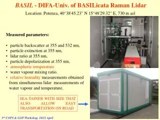
65nm test results :The tested chip : ATPIX65A, Atlas Pixel prototype array Small array of 16x32 pixels designed at Berkeley, using 65 nm CMOS process. Pixel area : 25 µm x 125 µm Pixel Configuration : 8 Triple Redundant Latch (TRL) with error correction Data loaded and read back with shift register (SR) . 16 columns of 256 Configuration TRL and 256 DFF Design based on standard cells from ARM library AIDA, 2nd annual meeting Frascati, April 10th 2013 4
65nm test results : SEU results • Test results : • Improvement by factor 4 compared to the FE-I4 configuration cell • TRL cell is 170 times more tolerant than a DFF 170 4 • Test conditions : • IRRAD3 beam line of the CERN Proton Synchrotron (PS) • Beam of 24 GeV protons with a spot area around 1 cm² • Reach a fluency of 1 - 3 1013 p/cm2 per hour • Data acquisition based on FPGA and synchronized with the spill signal • SEU rate is computed for the TRL (configuration cell) and for the DFF (shift register unit cell) AIDA, 2nd annual meeting Frascati, April 10th 2013 5
65nm test results :Dose effect • Chip 2 : irradiated up to 435 MRad (1 spill/cycle and annealing during 10-20 hours each 10-20 MRad) • Systematic errors start to appear from 350 Mrad. • These systematic errors are not SEU errors but it’s a dose effect. 350MRad AIDA, 2nd annual meeting Frascati, April 10th 2013 6 • At high levels of dose, systematic errors appear in the configuration memory. (The state of some DFF cells remains stuck to 0 or 1.) • 2 chips were irradiated with 24 GeV proton beam. • Chip 1 : irradiated up to 870 MRad (3 spill/cycle without annealing) • Systematic errors start to appear from 350 MRad. • Chip out of the beam : we still have errors but the number of errors decreases with annealing effect • Still have errors after 420 hours of annealing.
65nm test results :Dose effect on the 65nm device • The leakage current increases by 1 order of magnitude for a total dose of 435 MRad • No threshold voltage shift up to 100 MRad but more pronounced from 200 MRad • Narrower devices (W=150nm-200nm for digital) should show more shift on the threshold • More irradiation tests have to be done (Xray irradiation at CERN next week) • For Chartered 130 nm process Xray irradiation did not show such a high dose behavior observed with proton • Special layout rules have to be defined for digital cells when the TID have to exceed 200 MRad AIDA, 2nd annual meeting Frascati, April 10th 2013 7
AIDA 65nm designs in progress: Configuration Blocks AIDA, 2nd annual meeting Frascati, April 10th 2013 8 • Pixel configuration : • Good SEU results BUT for some very sensitive config bit (the MSB of threshold DAC …) the SEU tolerance should be improved. • A new design is under development with several flavors : • Triple Redundant Latch with delays • DICE latches • Global configuration : • Improve the SEU tolerance of the unit cell. • Minimize the effect of glitches (identify the sensitive nodes…) • Triplicate the Majority Logic • Correction with hamming code
AIDA 65nm designs in progress:Generic ADC for monitoring 10 bit SAR ADC Analog MUX out inputs Vin status en clk start select • General purpose ADC (collaboration with LAPP) • Inputs are slow variation signals: Temperature, leakage current … • Clock frequency : 100 kHz -1 MHz • Architecture : Successive Approximation Register (SAR) • Precision : 10 bit (12bit ? If required) • DC accuracy : • Integral linearity error : +/- 1 bit • Differential linearity error +/- 0.5 bit • Voltage Reference provided by an external IP block • Operating input voltage : 0-Vref • Conversion time : 12-14 clock cycles • Tolerance to a TID of 1000 MRad AIDA, 2nd annual meeting Frascati, April 10th 2013 9
AIDA 65nm designs in progress:BandGap reference Vdda Bg_outa en BGVR Bg_outb Gnda AIDA, 2nd annual meeting Frascati, April 10th 2013 10 BandGapReference for general purpose provide voltage reference for : Biasing, DAC, ADC … 2 Voltages : to be defined (0.8V? and 0.6V?) Temperature : from -50 °C to 120 °C Temperature coefficient : 400 ppm/°C max Voltage coefficient : TBD Start up circuit CLoad MAX = 20pF and RLoad = 10 MOhms Power supply = 1.2 V Power consumption Noise < 20 µV RMS Radiation hard : 1000 MRad
AIDA 65nm future design :Temperature Sensor Vbn Vdda out en TempSens Gnda AIDA, 2nd annual meeting Frascati, April 10th 2013 11 Precision : +/- 1 °C Functional temperature range -40 to +60 °C Sensitivity better than 0.6 mV/°C Radiation tolerance : 1000 MRad Correction of the irradiation effect
Conclusion • TSMC 65 nm process allows good tolerance to SEU. • However the tolerance of TSMC-ARM digital cells have to be investigated for high dose level : 1000 Mrad Dose effect : Simulations are in progress to check if there are “sensitive” devices inside the Library DFF cell. • New designs are in development : • different structures of configuration memories, • IP blocs : ADC, Voltage reference • First submission of 65nm CMOS IP blocks (plus individual narrow test transistors) is foreseen in June or September 2013. AIDA, 2nd annual meeting Frascati, April 10th 2013 12


![Nm]](https://cdn3.slideserve.com/6300766/slide1-dt.jpg)