Download
1 / 14
140 likes | 148 Vues
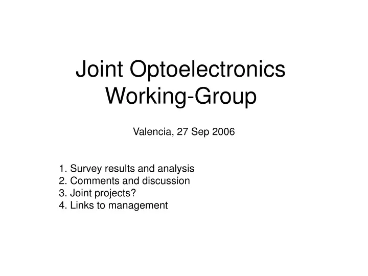
Joint Optoelectronics Working-Group. Valencia, 27 Sep 2006 1. Survey results and analysis 2. Comments and discussion 3. Joint projects? 4. Links to management. Proposed way forward 23 June 2006.

E N D
Joint Optoelectronics Working-Group Valencia, 27 Sep 2006 1. Survey results and analysis 2. Comments and discussion 3. Joint projects? 4. Links to management
Proposed way forward23 June 2006 • By Aug 31st, Institutes express their interest to participate to WPa.b and indicate their available resources • On Sep 27th (LECC06 Valencia), the work-packages which have reached critical mass and group two or more institutes can be launched • ATLAS and CMS Funding requests for optoelectronics R&D are commonly reviewed by WG members who sit in CMS or ATLAS SLHC review committees.
Joint Optoelectronics Working-GroupProposed Work-package Breakdown 3. Environment 3.1 Radiation hardness 3.2 Reliability 2. System layer 2.2 Demonstrators 2.3 Testing 2.1 Design and simulation 2.4 Interface to DAQ 1. Physical layer 1.1 Interface to front end 1.2 data collection 1.3 data transport 1.4 Interface to back end FE BE Optoelectronics working group
Academia Sinica (?) S.C Lee, TBD Ohio State University K.K. Gan, 1.5 FTE University of Oklahoma Oklahoma State University Patrick Skubic, 1.4 FTE Southern Methodist University Jingbo Ye, 8 FTE University of Ljubljana Igor Mandic, 0.3 FTE University of Oxford Cigdem Issever, 1.6 FTE CCLRC RAL Technology-ESD John Coughlan, 0.5 FTE CERN-PH-MIC Francois Vasey, 5 FTE Imperial College (?) Geoff Hall, TBD IN2P3-IRES Strasbourg Abdenour Lounis, 3 FTE Polytechnique LLR T. Romanteau, 1.2 FTE University of Minnesota (at CERN) R. Rusack, 0.5 FTE Joint Optoelectronics Working-GroupInterested Institutes CMS origin ATLAS origin 7 institutes, 12.8FTE 6 institutes, 10.2FTE
Joint Optoelectronics Working-GroupSurvey Results ATLAS+CERN 3. Environment 3.1 Radiation hardness Oxford, Ljubljana Oklahoma, Ohio, SMU CERN, Minnesota 3.2 Reliability SMU Oxford CERN CMS CMS 2. System layer 2.1 Design and simulation SMU Polytechnique (behavioral model) 2.2 Demonstrators Ohio SMU CERN (PON) 2.3 Testing Oxford IRES (test DAQ) CERN, Minnesota 2.4 Interface to DAQ Polytechnique (ACTA) RAL (ATCA) IRES 1. Physical layer 1.1 Interface to front end IRES (super hybrid) 1.2 data collection SMU (interface ASIC) CERN (Versatile bidi link) 1.3 data transport SMU (link on chip) Ohio (driver, receiver) Oklahoma, Ohio (tests) Taiwan (ASIC) IRES CERN (Versatile bidi link) 1.4 Interface to back end RAL (system on FPGA) Polytechnique (FPGA) FE BE
SMU Project Flipped OE devices on SoS substrate flip chip attachment UTSi integrated photo detector UTSi integrated circuitry receiver circuitry VCSEL driver circuitry quad PIN array quad VCSEL array active CMOS layer 200 um transparent sapphire substrate (UTSi) MMF ribbon fiber
CERN project proposal: Versatile Bi-directional Digital Link
Comments Please Joint Optoelectronics Working-GroupInterpretation of Survey Results • 13 institutes, 23 FTE • 3 institutes above 3 FTE: SMU (8), CERN (5), IRES (3) • 2 development projects announced: • Link on chip SOS (SMU, ongoing) • Versatile bidirectional link (CERN, proposal) • 10 institutes below 3 FTE (0.8 average) • Mostly involved in testing • Core activity: ex-ATLAS and CERN • Optoelectronics developments and testing • Periphery: ex-CMS • Hybrids, Backends, system modeling • No system level work
Proposal for a different operating mode, 23 June 2006 • Move from reporting to collaborating mode • Identify the areas of expertise of collaborators • Collaborate in smaller subgroups, organize topical meetings? • Prepare common R&D proposals? • Report at bi-yearly plenary meetings
Joint Optoelectronics Working-GroupPossible Sub Groups ? Environment 3.1 Radiation hardness Oxford, Ljubljana Oklahoma, Ohio, SMU CERN, Minnesota 3.2 Reliability SMU Oxford CERN Interfaces 2. System layer 2.1 Design and simulation SMU Polytechnique (behavioral model) 2.2 Demonstrators Ohio SMU CERN (PON) 2.3 Testing Oxford IRES (test DAQ) CERN, Minnesota 2.4 Interface to DAQ Polytechnique (ACTA) RAL (ATCA) IRES 1. Physical layer 1.1 Interface to front end IRES (super hybrid) 1.2 data collection SMU (interface ASIC) CERN (Versatile bidi link) 1.3 data transport SMU (link on chip) Ohio (driver, receiver) Oklahoma, Ohio (tests) Taiwan (ASIC) IRES CERN (Versatile bidi link) 1.4 Interface to back end RAL (system on FPGA) Polytechnique (FPGA) FE BE Components and system
Joint Optoelectronics Working-GroupPossible Collaborative projects ? • Test procedures and metrics • Test equipment and facilities • System level test beds • Opto-system specifications and interfaces • Connectivity to front and back-end • … • Or crystallize around announced projects
Joint Opto Group ↔ ATLAS/CMS/CERN Upgrade Management ATLAS: Upgrade Steering Group & Upgrade Project Office CERN CMS: Upgrade Steering Group Joint Opto Group: ATLAS CMS CERN • Inclusion of Joint Opto Group into upgrade managements? • Review of joint proposals? Submit to three review panels? • Can we simplify ?