Download
1 / 47
480 likes | 682 Vues
Presented by Julien Mekki IES , University Montpellier II, France CERN , Geneva, Switzerland. Radiation damage to electronic devices for LHC and Super-LHC experiments. Seminar IPNL – Lyon – France 14 th January 2011. Outline. I. Introduction

E N D
Presented by JulienMekki IES, University Montpellier II, France CERN, Geneva, Switzerland Radiation damage to electronicdevices for LHC and Super-LHC experiments Seminar IPNL – Lyon – France 14th January 2011
Outline • I. Introduction • II. Packaging effect on RadFET sensors for the radiation monitoring • project • III. Forward biased p-i-n diodes used as dosimeters • IV. Perspectives and outlook on future studies • V. Conclusion
Who am I ? • Actual position • Assistant professoratUniversity of Montpellier 2 – CERN USER. • Study of silicon detector performances for LHC and Super-LHC experiments. • PhD in Electronics (Nov. 2009) – (CERN, Université Montpellier 2) • Characterization and performance optimization of radiation monitoring sensors for highenergyphysicsexperimentsat the CERN LHC and Super-LHC • Master thesis in Science and Technology (2006) (CNES, EADS Astrium) • Radiation hardness of electronic components used for space applications. • February 2011: • Senior fellowat CERN – EmergingEnergy Technologies department • Project: Radiation to electronics (R2E)
Balloon (30 Km) CD stack with 1 year LHC data! (~ 20 Km) Concorde (15 Km) Mt. Blanc (4.8 Km) CERN Technologies • Three keys technologies at CERN Accelerating particle beams Detecting particles GRID Large-scale computing (Grid)
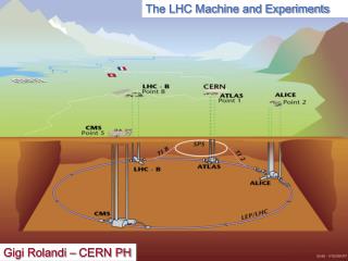
CMS The Large Hadron Collider (LHC)
The Large Hadron Collider (LHC) • Mixed radiation field • Hadrons (n, p, k+,k-, π+, π-) • Leptons (e-, e+, μ-, μ+) • Photons • Intense close to the interaction point ATLAS • General design principle • Sub-detectors: • Inner detectors → Trackers • Calorimeters → Energy deposited • Muon gas chamber 7 TeV 7 TeV
Radiation monitoring project – Why ? • The effect of radiation on electronic and detector components → Major issue • All equipments → Affected by radiation damage • LHC experiments are designed to operate for 10 years. • → Radiation level survey needed for damage and failure analysis. • Different radiation field parameters have to be monitored… Different sensitivity and range are required… Different small active devices have been investigated !
Radiation monitoring project – What ? • Ionizationeffect • TID (Total Ionizing Dose) • e.g. accumulation of charge in SiO2 : damage to microelectronic components • Unit Gray: 1 Gy = 1 Joule released in 1 kg of matter = 1 J/kg ATLAS • Non-Ionizatingeffect • NIEL (Non Ionizing Energy Loss) • causinge.g. crystaldefects in semiconductorcrystals: silicon detector damage • Unit: 1 MeV neutrons/ cm2 “equivalent fluence” (Фeq) • Luminosity: 1034cm-2.s-1 • Ideal: Measure the full radiation spectrum (particle type, energy and intensity at all locations) • → Impossible (there is no such device) • In space (Geostationary orbit) 10-30 Gy/y
Radiation monitoring project – How ? • Many radiation sensors tested, only few of them was selected and installed in • the LHC experiments • 2 major issues: • Measure of the TID • Measure of the 1-MeV Фeq 2 types of RadFET: 250 nm oxyde thickness → REM,UK 1600 nm oxyde thickness → LAAS, France BPW34 Commercial Silicon p-i-n diodes
Radiation monitoring project – How ? • Many radiation sensors tested, only few of them was selected and installed in • the LHC experiments • 2 major issues: • Measure of the TID • Measure of the 1-MeV Фeq 2 types of RadFET: 250 nm oxyde thickness → REM,UK 1600 nm oxyde thickness → LAAS, France BPW34 Commercial Silicon p-i-n diodes • Packaging can induce possible dose enhancement in the measurements. • The only freedom remaining in the design is the chip carrier cover. • But, like the chip carrier, it has an effect on the TID measurement.
Packaging effect on RadFET sensors for the radiation monitoring project
RadFETs General • e-/h+ pair generation; • e-/h+ pair recombination; • e- / h+ transport; • hole trapping; • Interface state. Build-up of charge in SiO2 increase of the p-MOS Threshold Voltage integrated Dose Measurement Exposure: “zerobias” Readout: iDS VGS ∝ TID
γ-neutron Irradiation • Chip carrier was placed into the reactor core • Various materials and thicknesses • Measurement: dose Slight increase of TID was measured for thicknesses exceeding 1 mm. Ref : F. Ravotti. Phd thesis, University Montpellier II, France.
Packaging Effect on RadFET sensors • How the RadFETs response is influenced by the cover ? • and also …. • How much doseis deposited by different particles with different energiesin the RadFETs ? • RadFET response studied using the simulation toolkit:
What is GEometryANdTracking • C++ based / Object Oriented Toolkit for the simulation of particle interactions with matter. • Geant4 provides the possibility to describe accurately an experimental setup. • (Geometry and Materials) • The program provides the possibility of generating physics events andefficiently track particles through the simulated detector. • The interactions between particles and matter must be simulated by taking into account all possible physics processes, for the whole energy range.
With ceramic cover Geant4 Model • Chip carrier has been hit perpendicularly in the front side. • Result of the simulation is the total energy deposited by primary and secondary particles. • First set of simulation: • → Full dies size are taken as sensitive volume • Second set of simulation: • → sensitive volume: thin oxide Layer (SiO2) Without cover Packaging REM-TOT-500 LAAS-1600
Packaging comparison • Results for Pions: • Charged hadrons are dominated by pions close to the interaction point. • Most important contribution on the total energy deposited in a mixed field. • Low energy pions are absorbed in the cover. • Simulation have been carried out for all particles and energies present in the LHC radiation field.
1 RadFET sensors in the ATLAS detector • Provide information about the TID in the LHC experiments 2 • 2 locations are taken as example: • Inner detector (1) • Liquid Argon Calorimeter (2) • 260 µm cover has been investigated and compared to uncovered RadFETs • Estimation of the total energy deposited in the RadFETs as well as the cover effect for each particle type. • 18
Results • Detailed results for the Inner Detector : • About 45 % of the energy is deposited by pions. • Significant dose enhancement for photons due to secondary particles. • Photons deposit less than 2 % of the overall energy. • 19
Results • Pions: • Pions are charged hadrons: heavy particles • Mass 270 timeshigher than e-. • Energy deposited → Bragg peak Energy deposited in the medium (MeV.cm-2.g-1) • Bragg peak Depth (cm) • Photons: • Secondary particles (e-, e+) • → Compton, pair production effects • → Photonuclear absorption (α) Alpha (e-; e+) Compton e-
Results • Results for the Liquid Argon Calorimeter: • Total Dose enhancement = 23.6 ± 2.4% • Pions represent 0.1 % of particles → contribution to dose ≈ 7 % • Protons deposit about 35%of the overall energy • (represent only 0.08 % of particles, but mass 1800 times higher than e-.) • Annual dose values in the covered and uncovered RadFET sensors for both locations.
Conclusion of this study • Dose enhancement as TID was simulated using Geant4 for all particles and energies present within the LHC radiation field. • Understanding of each particle and energy influence. • 260 µm thick Alumina cover can alter the measured dose up to 25 %. • The choice of RadFET packages is thus important for measuring the TID in High Energy Physics Experiments. • Study published in J. Mekki et al, IEEE TNS, vol. 56, no. 4, pp. 2061-2069, 2009.
Radiation Monitoring at the LHC Experiments • 2 major issues: • Measure of the 1-MeV Фeq • → 108 ≤ Фeq ≤ 1014 -1015 neq/cm2 for LHC • Measure of the TID 2 types of RadFET: 250 nm oxide thickness → REM,UK 1600 nm oxide thickness → LAAS, France BPW34 Commercial silicon p-i-n diodes
VF iF p-i-n diodes (NIEL) • Displacement damage in high r Si-base • Resistivity increases vs Фeq FORWARD BIAS Fixed IF VF Фeq VF = (material parameters, geometry [W], readout current [J], pulse length) BPW34 p-i-n diode: Thickness ≈ 300 µm, Area =2.65×2.65 mm2, ρ ≈ 2.7 kΩ.cm
Readout protocol for LHC BPW34 diode FORWARD BIAS Fixed Readout Current IF VFФeq IF = 1 mA with a short duration pulse • F. Ravottiet al., IEEE TNS, vol. 55, no. 4,pp. 2133-2140, 2008 • Hadron sensitivity range from 2×10¹² to 4×10¹⁴neq/cm2. • Perspectives for the future Super-LHC: • Luminosity and radiation level (×10). • Detectors will be exposed to fluences up to 1016 1-MeV equivalent neutrons. • A solution to measure very high fluences has to be found
First study • New readout protocol • Different current steps of 50ms pulse duration • Current used: 10µA – 100µA – 1mA – 5mA – 10mA – 15mA – 25mA Increase of bulkresistivitywithФeq • Thyristor - like behavior (F. Ravotti et al, IEEE TNS, vol. 55, no. 4, pp. 2016-2022, 2008.) • Self-heating of the diode
Second Study • Detailed study of the detectors behavior Development of 2 tests benches for the detector characterization Modifications of the electrical properties of the material
Second study(1/2) • I-V curves from very low voltages (=1mV), to high voltages. • Up to 6.26×10¹⁵ neq/cm2(60% of the expected Super-LHC fluences) 2 differents regimes can be distinguished: First regime: • At low fluences: • At low voltages a linear region can be observed. • As VF increases: linear region → sharp increase of IF. Forwardcurrent (A)
Second study (2/2) Forwardcurrent (A) Rise of IF vs Фeq increases up to ≈ 1 × 10¹³ neq/cm2 Second regime: • For Фeq> 1 × 10 13 neq/cm2, I-V characteristics are linearatlow voltages. • Withfurtherincrease of the radiation level, thislinearbehaviourextend to higher VF.
New formulation (1/3) • This new formulation is based on the relaxation material theory • Relaxation materials have a large density of g-r centers near Eg/2. • Recombination pins the fermi level at minimum conductivity • Maximum resistivity: Фeq Forwardcurrent (A) • (see references in my PhD thesis) • http://jmekki.web.cern.ch/jmekki/2009-11-27-Thesis-Mekki.pdf
New formulation (2/3) • Relaxation materialswereexperimentallyfitted as : Фeq = 6.3×10¹⁴ neq/cm2 Фeq = 6.3×10¹⁵ neq/cm2 IF ≤ 1mA IF ≤ 1mA IF ≥ 1mA IF ≥ 1mA Forward current (A) Forward current (A) FIT FIT • For IF > 1mA, possibility to have thyristor-like behavior1 and/or self-heating effect. • 1F. Ravottiet al., IEEE TNS, vol. 55, no. 4,pp. 2133-2140, 2008
New formulation (3/3) • At the LHC experiments, BPW34FS diodes are operated in forward bias. • A new formulation to predict and monitor values of VF versus Фeq: • For Фeq ≥ 1×10¹³ neq/cm2 • For IF ≤ 1mA • Based on: IF = 1 mA LambertW(x) function is the inverse function of: IF = 100 μA IF = 10 μA
Qualitative evaluation of the temperaturedependence • Temperature Coefficient < 0 • ni increases with T°, so ρmax decreases when T° increases.
Conclusion of thisstudy • Effects on radiation damage up to 6.3×10¹⁵ neq/cm2on the OSRAM BPW34FSsilicon p-i-n diode have been studied. • Comparisonwithrelaxation materials. • New formulation to predict VF versus Фeq for: • Фeq ≥ 1×10¹³ neq/cm2 • IF ≤ 1mA • Sensitivityisincreased, and Фeqmeasurement range canbeexpandedwhen diode ismeasuredatlowertemperature. • Summary: • Allow to extend the existingreadoutprotocol. (IF = 1 mA) • Permit to predict radiation response for expected SLHC fluences. • Study published in J. Mekki et al, IEEE TNS, vol. 57, no. 4, pp. 2066-2073, 2010.
Perspectives and outlook • BPW34 p-i-n diode can be used for monitoring LHC and Super-LHC fluences from 2×10¹² neq/cm2. • 2 possibility already exists: • → Pre-irradiation allows to measure Фeq > 8×10⁹ neq/cm2. • → CMRP diode (Thickness = 1 mm; Area = 1.2 mm2, ρ ≈ 10 kΩ.cm): • 1×10⁸ < Фeq (neq/cm2 ) < 2×10¹² • With the intention to develop our specific dosimeter • → An investigation on custom made devices (high resistivity silicon detector)
Silicon Detectors • Tested devices were made from n-type FZ and MCz silicon wafers. • Geometry dependence on the detector’s radiation response has been evaluated. • → 2 different active area: 2.5×2.5 cm2 and 5×5 cm2 • → 2 different thicknesses: 300 µm and 1000 µm • Outcome: • The device thickness is the main parameter which influence their radiation response.
Silicon Detectors Sensitivity isincreased by a factor ≈ 25 Thin detector Thick detector • Study published in J. Mekki et al, IEEE TNS, vol. 57, no. 6, pp. 3483-3488, 2010.
Silicon Detectors Sensitivity isincreased by a factor ≈ 25 Фeq ≈8×10¹² neq/cm2 Thick detector Фeq =2×10¹² neq/cm2 Thin detector Фeq =2×10¹⁰ neq/cm2 Thick detector • Study published in J. Mekki et al, IEEE TNS, vol. 57, no. 6, pp. 3483-3488, 2010.
General Conclusion • Monitor the LHC radiation field: 2 devices • → RadFET (TID) • → p-i-n diodes (Фeq) • RadFETs: • Evaluation of packaging configurations • Evaluation of the TID and package impact on a real LHC experiment. • → Dose enhancement up to 25 % • p-i-n diodes: • New formulation for monitoring very high fluences (Super-LHC). • At low temperature → expand to higher fluences • Custom made devices : • Sensitivity for low Фeq can be improve using thicker p-i-n diodes or detectors.
Thankyou for your attention Thankyou for your attention The Atlas Detector • 42
Self heating effect • Normal readout protocol: • Wait for temperature stabilization inside the diode after each measurement: • Outcome: • Problem for measuring at high injection level due to self-heating. Self heating VF at IF = 1mA VF at IF = 100µA VF at IF = 25mA Measurement Self heating 50ms 50ms 50ms • After measurement • VF2 < VF1(self-heating) • Wait intil VF2=VF1 50ms 50ms VF at IF = 10µA VF at IF = 10µA VF at IF = 10µA 50 ms VF1 at IF = 10µA VF2 at IF = 10µA
Summary of the relaxation materialstheory (1/3) • Relaxation theoryoccurswhen the material has highresistivity, and containsdefects due to impurities or damage whichenhance the G-R rate. • Definition of the dielectric relaxation time: • Time to restore charge neutrality to a regionwhenexcess carrier are suddentlyintroduced. • Whenexcess carriers are injectedacross the PN junction, at the instant of injection (t=0), therewillbe an excess charge (Δn,p) , sothat charge neutralityisdisturbed. • It isassumed to be the bulkequivalent of a RC time constant : • τD = ρεε0
Summary of the relaxation materialstheory (2/3) • Example: Injection of minority carriers in the n side (Δp): At t = 0 → there are excess holes but no excess e- Diffusion of holes (gradient of holes) e- (Δn) are attracted in this region by drift because of the field induce by Δp. Δn flow in from the contact to neutralizeΔp This neutralizationoccurs in a dielectric relaxation time (τD). • Whileneutralityisquicklyestablished, Δp diffuse slowly and recombine with e-sothatthereisstillexcess charges in the material :The conventionnal carrier lifetimeτ0 • Resistivityisdecreased by the enhancement of carrier in the material. • In conventionnallifetimematerial, neutralityisrestoredbeforeexcess carrier recombine. τ0 >> τD • The np productisequal to: np = ni2×exp[(Фn-Фp)/kT];Фn and Фp are the quasi-fermi levels for e- and h+ , and isdependent on the applied voltage.(V =Фn-Фp) n(x) p(x) p(x) n(x) n0 Δp Δn Δp p0 p0 n0 x x x x
Summary of the relaxation materialstheory (3/3) • For irradiated diodes, the materialbecomeshighly recombinative do to highdensity of recombinationcenters. • Minority carrier injection increases the resistivitysince the concentration of minority and majority carriers isreduced by recombination. τD = ρεε0 increases. τD >> τ0 • Injectedminority carrier lead to a depletion of majority carriers through the g-r centersactivity. Therefore the carrier equilibriumisrapidlyreached → no possible to influence it by externallyapplied voltage. • Recombination pins the fermi level at minimum conductivity (defect near Eg/2) • → np = ni2 as for the steady-state condition in lifetime diode. • Maxiumum resistivity of Silicon :