Download
1 / 24
240 likes | 387 Vues
Low Cost FPGAs. March 2006. LatticeECP2 – Low Cost & High Performance. Low Cost, LUT-based FPGA 6K to 70K LUT4s 12K to 136K bits distributed memory 95 to 628 I/O High volume prices as low as $0.50 per 1K LUTs Flexible sysIO TM Buffers LVCMOS 33/25/18/15/12, PCI

E N D
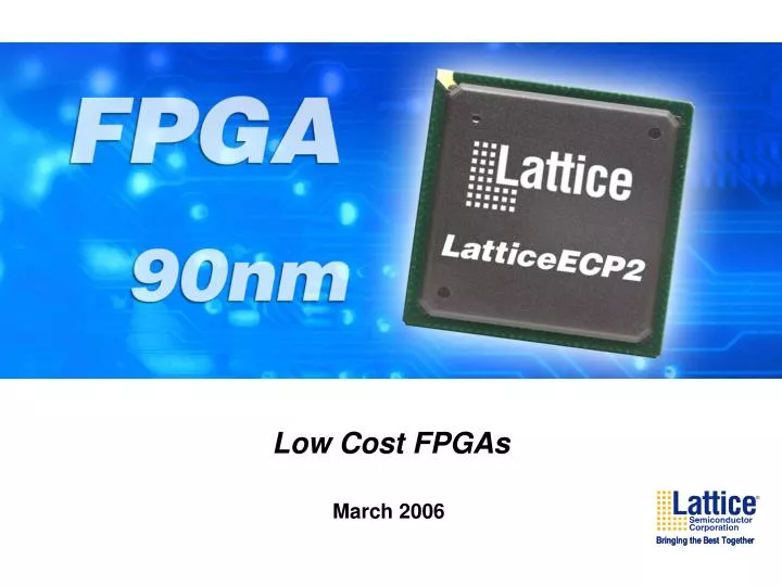
Low Cost FPGAs March 2006
LatticeECP2 – Low Cost & High Performance • Low Cost, LUT-based FPGA • 6K to 70K LUT4s • 12K to 136K bits distributed memory • 95 to 628 I/O • High volume prices as low as $0.50 per 1K LUTs • Flexible sysIOTM Buffers • LVCMOS 33/25/18/15/12, PCI • SSTL3/2/18 & HSTL15 & HSTL18 • Bus-LVDS, MLVDS, LVPECL & LVDS • Pre-engineered Source Synchronous I/Os • DDR2 (400Mbps) • sysDSPTM High Performance DSP Support • 12 to 88 18x18 multipliers • sysMEMTM Block Memory • 55K to 1M bits • sysCLOCKTM PLL and DLL • Enhanced Configuration Support • Configuration bitstream encryption • Transparent updates • Dual boot support Low Cost 840Mbps Parallel I/O Bitstream Encryption 28 GMAC DSP 400Mbps DDR2
LatticeECP2 – Architecture Flexible sysIO Buffers: LVCMOS, HSTL,SSTL, LVDS, ++ Programmable Function Units (PFUs) Pre-Engineered Source Synchronous Support DDR2 – 400Mbps Generic – 840Mbps DSP Blocks Multiply and Accumulate Support sysMEM Block RAM 18kbit Dual Port Flexible Routing Optimized for Speed, Cost and Routability sysCLOCK PLLs & DLLs Frequency Synthesis & Clock Alignment Config. Logic Inc Dual Boot, Encryption & Transparent Updates On-Chip Oscillator Configuration Port
Optimized Programmable Function Unit (PFU) Carry Chain • PFU Resources Optimized • Best match to applications • Best speed • Best cost • Tools Tuned To Optimally Use Available Resources SLICE 3 LUT4 LUT4 SLICE 2 LUT4 FF LUT4 FF From To Routing Routing SLICE 1 LUT4 FF LUT4 FF SLICE 0 LUT4 FF LUT4 FF 1. Available in 25% of the PFUs Logic Block (PFU) Carry Chain
Extensive High Performance Clocking • High Performance Clock Distribution • Eight global clock networks • Eight regional secondary clocks • Two low-skew edge clocks per side • sysCLOCK PLL and DLL Technology • 2 to 6 PLLs per device • External capacitor allows operation as low as 1MHz • Dynamic phase shift capability • 2 DLLs per device • Includes slave delay for source synchronous implementations • On-Chip Oscillator (Typ 130MHz) • Edge Clock Divider • X2, X4, X8 • For high speed source synchronous implementations
sysCLOCK PLL Dynamic Adjust Dynamic Adjust PLL Input Clock Divider (CLKI) LOCK CLOCK IN (From pin or routing) Phase & Duty Select Post Scalar Divider (CLKOP) Delay CLOCK OUT Adjust* Feedback Divider (CLKFB) Feedback (From post scalar divider, clock net or external pin) CLOCK OUT Secondary Clock Divider (CLKOK) +/- 8 Steps 130ps Nominal CLOCK OUT * GPLL Only Optional External Capacitor • Two General Purpose PLLs (GPLLs) Per Device • Up To Four Standard PLLs (SPLLs) Per Device • Frequency Range 1 to 420MHz • Programmable Phase / Duty Cycle (22.5 degree steps) • Programmable Dividers • Internal and External Feedback • PLLs Filter Jitter
sysCLOCK DLL • Flexible DLL Provides 3 Modes: • Calibrated delay • Clock injection removal • Clock match • 100 to 500MHz Operation • DLLs Maintain Clock and Data Alignments sysCLOCK DLL Output Mux Clock Out 50% Duty Cycle Phase Comparator Clock In (From pin or routing) 2/4 Clock Out 50% Duty Cycle Feedback (DLL Internal, clock net or external pin) Delay Line ALU Lock Matched Delay Delay Line Clock In (From pin or routing) Clock Out Note: Simplified diagram
On-Chip Oscillator Provides Low Cost Clock Ideal for non-timing-critical state machines Drives Internal Routing Can be routed off chip Nominal Frequency Can Be Set 2.5 to 130Mhz Easily Implemented With ispLEVER Design Tools On-Chip Oscillator OSCD OSC Oscillator Primitive COMPONENT OSCD -- synthesis translate_off GENERIC (NOM_FREQ: string := 2.5); -- synthesis translate_on PORT (OSC:OUT std_logic); END COMPONENT; attribute NOM_FREQ : string; attribute NOM_FREQ of OSCins0: signal is “2.5”; Example VHDL Usage
High-Performance sysDSP Block • Programmable Multiplier • One 36x36 or four 18x18 or eight 9x9 • Programmable Addition, Subtraction & Accumulate • Programmable Pipelining • Input / Intermediate / Output • 325MHz Performance • Provides up to 28.6 GMAC/second per device • Suitable For Wide Range of DSP Functions Including • FIR Filters, FFTs and complex arithmetic sysDSP Block X +- X + X +- X
Pre-Engineered Source Synchronous I/O DDR to SDR Conversion • Implement High Speed Memory Interfaces • DDR1/2 • Implement High Speed Source Synchronous Interfaces • SPI4.2 • ADC/DAC • Pre-Engineered I/O Logic Support • DDR to SDR conversion • Gearbox logic • DQS/Strobe alignment PIC PIO A Tri-state Register Block (2 Flip/flops) 2:1 Gearbox (Optional) Shared With PIO B Output Register Block (2 Flip/flops) Input Register Block (5 Flip/flops) Input DQS/Strobe Delay and Transition Detect* PIO B (Detail Not Shown) * Selected blocks 2:1 Gearbox For Operation Up to 840Mbps Precision Strobe/DQS Alignment
sysIO Support sysIO Buffer Support Chip Level Support * Includes PCI clamping diode. Bottom I/Os only ** HSTL II outputs only supported for 1.8-volts *** Drivers on 50% of pairs left and right side of the device only **** LVPECL and BLVDS can be supported through emulation
LVCMOS/LVTTL I/O Features • Hotsocketing Capable • Input leakage less than 1mA during power-up/power-down • Power supplies can be sequenced in any order • Programmable Slew Rate • Programmable Drive Strength • 4 to 20mA (3.3-volts) • 4 to 20mA (2.5-volts) • 4 to 16mA (1.8-volts) • 4 to 8mA (1.5-volts) • 2 to 6mA (1.2-volts) • Programmable Pull-up, Pull-down, Bus-friendly • Programmable Open Drain
I/O Banking Scheme V V V V V V GND GND • Eight General Purpose I/O Banks Per Device • Configuration pins in separate bank • Output Standard Support Dependent on VCCIO • Referenced Inputs Dependent on VREF • LVCMOS Inputs • 12, 25 & 33 independent of VCCIO • 15 & 18 dependent on VCCIO • Multiple Compatible I/O Standards In A Bank CCIO0 CCIO1 REF2(0) REF2(1) REF1(1) REF1(0) Bank 0 Bank 1 V CCIO2 V REF1(2) V Bank 2 CCIO7 V REF2(2) V REF1(7) Bank 7 GND V REF2(7) GND V CCIO3 V REF1(3) Bank 3 V CCIO6 V REF2(3) V REF1(6) GND Bank 6 V REF2(6) V GND CCIO8 Bank 8 GND Bank 5 Bank 4 REF2(5) REF1(5) CCIO5 REF2(4) REF1(4) GND CCIO4 GND V V V V V V
Soft Error Detect (SED) Logic • LatticeECP2 Devices Contain Hard SED Logic • Not available in Spartan/Cyclone • Checks Configuration Bits In Background • Compares to CRC • Ignores EBR and distributed memory • In Case of Error Optionally: • Generates an error flag • Background reconfigures logic • Initiates a full reconfiguration • Target This Feature for High Reliability Applications • SED is a “non-issue” for most applications LatticeECP2 Configuration Bits Configuration Logic Hard SED Logic
Encryption Decrypted Data Configures FPGA LatticeECP2 Configuration Memory Decryption Engine 128-bit Key In OTP Non-Volatile Memory 128-bit AES Encrypted Bitstream 128-bit Key • Design Security Increasingly Important • Overbuilding, reverse engineering and cloning all too common • Encrypt Bitstreams With 128-bit AES Using ispVM • On-Chip OTP 128-bit Decryption Key Storage • Choose your own unique key • On-Chip 128-bit AES Decryption Engine
Dual Boot Mode SPI Configuration Memory LatticeECP2 Read Data Golden (A) Configuration Sector 0 Active (B) Configuration Sector 1 Control • Store Active and Backup (Golden) Configurations In SPI Configuration Memory • LatticeECP2 Will Automatically Use Golden Configuration If Active Configuration is Invalid • Increase System Reliability When Configurations are Field Updated LatticeECP2 Loads Active Configuration (B) at Power Up. If This Fails Configuration A is Used
TransFR I/O For Live Field Updates Step 2 Lock The I/Os In The Desired State Step 3 Apply New Configuration Step 4 FPGA Regains Control of I/O Step 1 Load New Config. To Configuration Memory Config. Memory Config. Memory Config. Memory Config. Memory (Config. 2) (Config. 2) (Config. 2) (Config. 2) LatticeECP2 LatticeECP2 LatticeECP2 LatticeECP2 Field Update FPGAs and Maintain High System Uptime Config. 1 Config. 1 Config.2 Config.2
Support Designs Over 300MHz * Simple functions (For example 16-bit decoder, 16-bit counter)
ECP2 Timeline • Family Publicly Announced, Collateral Available Now • Limited ECP2-50 Prototypes Available Now • Broad sample availability during Q2 • Whole family planned for production by the end of 2006 • Pricing As Low As $0.50 Per KLUT • Lowest speed grade, highest volume • ECP2-50 Supported in ispLEVER 5.1 SP2 • Extensive IP Support Planned For 2006
Advanced Configuration Support • Flexible Configuration Options • Low cost SPI boot memory, microprocessor, JTAG • Encrypted Bit Stream • On-chip 128-bit AES decryption • Encryption key securely stored on-chip • Automatic SPI Dual Boot • Allows recovery if power or communication fails during field update • Simple Field Configuration • Define I/O state during field configuration • Reconfigure FPGA while system operates
LatticeECP2 Competitive Comparison Exceptional Performance Uncommon Value