Download
1 / 21
210 likes | 217 Vues
Towards picosecond time measurement using fast analog memories D.Breton & J.Maalmi (LAL Orsay), E.Delagnes (CEA/IRFU). Why picosecond time measurements? for Time Of Flight (TOF) detectors in High Energy Physics >> to identify particles (detector goal ~ 25 ps rms)

E N D
Towards picosecond time measurement using fast analog memories D.Breton & J.Maalmi (LAL Orsay), E.Delagnes (CEA/IRFU)
Why picosecond time measurements? for Time Of Flight (TOF) detectors in High Energy Physics >> to identify particles (detector goal ~ 25 ps rms) Medical Imaging : Positron Emission Tomography (PET) >> Time of flight information reduces noise in image … Introduction • Goal: measuring the arrival time of fast pulses or time distance between two pulses with a precision better than 10 ps at high scale and low cost For a few channels, just buy a high-end oscilloscope !
State of the art • Existing electronics for time measurement based on Constant Fraction discriminators (CFD) associated with Time to Digital Converters (TDC). • Time resolution of ASICs based on CFDs (no time walk): ~ 30 ps • Pb : one cannot implement a pure delay line in an ASIC. • TDC with voltage ramp: best solution for resolution (~ 10 ps) • Usually used with a Wilkinson ADC for power and simplicity reasons => limited by dead time which can be a problem for high rate experiments • TDC with digital counters and Delay Line Loops (DLL): ~ 25 ps • advantage: produces directly the encoded digital value • Reminder: overall timing resolution is given by the quadratic sum of the discriminator and TDC timing resolutions => > 30 ps • Digital treatment of the digitized signal: • ADCs > 1GS/s => power, output data rate, need of high-end FPGAs • High Speed Analog Memories: low cost with very low power consumption
Why Analog Memories ? • Analog memories look like perfect candidates for high precision time measurements: • They catch the whole signal waveform • There is no need for precise discriminators • TDC is built-in (position in the memory gives the time) • Only the useful information is digitized (vs ADCs) • Any type of digital processing can be used • Only a few samples/hit are necessary => this limits the dead time • Simultaneous write/read operation is feasible, which removes the dead time if necessary • But they have to be carefully designed to reach such a high level of performance …
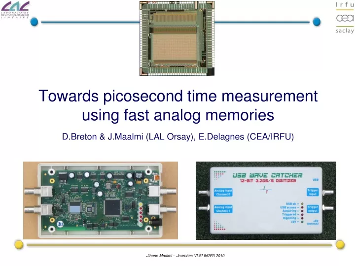
The USB WaveCatcher board The goal of the study is build a TDC working directly on analog pulses! Pulsers for reflectometry applications Reference clock: 200MHz => 3.2GS/s Board has to be USB powered => power consumption < 2.5W 1.5 GHz BW amplifier. µ USB Trigger input 2 analog inputs. DC Coupled. Trigger output +5V Jack plug Trigger fast discriminators Analog Memory (evolution from SAM) Cyclone FPGA Dual 12-bit ADC
Jitter sources and calibration • Jitter sources are : • Noise : depends on the bandwidth of the system • converts into jitter with the signal slope • Sampling jitter : due to clock Jitter and to mismatches of elements in the delay chain. • => induces dispersion of delay durations • 2.1 Random fluctuations : Random Aperture Jitter(RAJ) • - Clock Jitter + Delay Line • 2.2 Fixed pattern fluctuations : Fixed Aperture Jitter(FPJ) • => systematic error in the sampling time • => can be corrected thanks to an original method based on a simple 70MHz/1.4Vp-p sinewave (10,000 events => ~ 1.5 min/ch)
Noise Time Time Jitter Jitterinduced by electronics noise Simplified approach slope = 2ЛAf3db tr ~ 1/(3 f3db) Zoom Jitter [ps]~Noise[mV] / Signal Slope [mV/ps] ~tr / SNR Ex: the slope of a 100mV - 500MHz sinewave gets a jitter of ~2ps rms from a noise of 0.6mV rms • Conclusions: • The higher the SNR, the better for the measurement • A higherbandwidthfavours a higherprecision (goeswithits square root). • But: for a given signal, itisnecessary to adapt the bandwidth of the measurement system to that of the signal in order to keep the noise-correlatedjitter as low as possible • Designs becometricky for ultra fastsignalswith a bandwidth > 1GHz …
Fake signal Δt[cell] Real signal After interpolation Effects of the Fixed Pattern Jitter • Dispersion of single delays => time DNL • Cumulative effect => time INL. Gets worse with delay line length. • Systematic & fixed effect => non equidistant samples (bad for FFT). • We can measure it => we can correct it ! In a Matrix system, DNL is mainly due to signal splitting into lines => modulo 16 pattern if 16 lines • => correction with polynomial interpolation => good (and easy) calibration required.
Time calibration Method: search ofzero-crossingsegments of a sine wave =>length[position] Length[position]is proportional to time step duration assuming that: sine wave is a straight line (bias ~ 2ps rms). Sine wave characteristics: 70MHz -1.4Vpp Higher frequency => may be bothered by slew rate Lower frequency => lower slope => more jitter because of noise Histogram ofLength[position]: Mean_Length[position]: Fixed Pattern => DNL => INL Sigma_Length[position]:Random effect => Random Jitter
Jitter calibration Clock jitter 1.95ps rms Random jitter DLL jitter Corrected INL Raw INL DNL 16.9ps rms 1.5ps rms 7.5ps rms Integration Calibration The INL correction is stableover a long period of time (months …) => constants are stored in the on-board EEPROM
Characterization of time measurement. Open cable USB Wave Catcher USB Wave Catcher For the poor man … Two pulses on different channels Two pulses on the same channel => with this setup, we can measure precisely the time difference between the pulses independently of the timing characteristics of the generator!
CVI acquisition software with GUI This software can be downloaded on the LAL web site at the following URL: http://electronique.lal.in2p3.fr/echanges/USBWaveCatcher/
Source: asynchronous pulse sent to the two channels with cables of different lengths. Time difference between the two pulses extracted by CFD method. Threshold determined by polynomial interpolation of the neighboring points. Time measurement results. Spline and normalization Threshold interpolation 9.64ps rms Ratio to peak 0.23 Time 0.23 σΔt ~ 10ps rms jitter for each pulse ~ 10/√2 ~ 7 ps ! Other method used: Chi2 algorithm based on reference pulses.
Application: characterization of MCP-PMTs To test the adequation of 10µm MCPPMTs for time of flight measurements Original setup: beam at Fermilab => ~40pe at low gain (2-3 104) Beam CFD with walk correction Raw CFD measurement
New setup: MCP-PMT laser test at SLAC Same conditions as for Fermilab test: 40pe and low gain (2-3 104) 100Hz Digital CFD method TARGET board
SLAC test summary Sampling period! From this we could conclude that applying a very simple algorithm, which is very simple to integrate in a FPGA (finding a maximum & linear interpolation between two samples, i.e., without a use of the Spline fit) already gives very good results (only 10% higher than the best possible resolution limit). Summary of all the test results
NIM paper has been submitted in April Abstract:… There is a considerable interest to develop new time-of-flight detectors using, for example, micro-channel-plate photodetectors (MCP-PMTs). The question we pose in this paper is if new waveform digitizer ASICs, such as the WaveCatcher and TARGET, operating with a sampling rate of 2-3 GSa/s can compete with 1GHz BW CFD/TDC/ADC electronics ... … Conclusion: … The fact that we found waveform digitizing electronics capable of measuring timing resolutions similar to that of the best commercially-available Ortec CDF/TAC/ADC electronics is, we believe, a very significant result. It will help to advance the TOF technique in future.
Conclusion • The USB Wave Catcher has proven that analog memories can be used as analog TDCs at the ps scale. • Lab timing measurements showed a stable single pulse resolution < 10 ps rms • We are waiting for the new chip we submitted last April • CMOS 0.35µm, 2 channels, 1024 cells/channel • We hope to reach 5ps in the next timing-optimized chip (0.18µm) • The board has been tested with MCPPMT’s for low-jitter light to time conversion • Double pulse resolution ~ 23 ps => single pulse resolution ~ 16 ps • Even the simplest CFD algorithm can give a good timing resolution < 18 ps • It can be easily implemented inside an FPGA (our next step) • We are currently designing a 16-channel system for TOF measurement on the SLAC Cosmic Ray Telescope (September 2010) • Bandwidth, sampling frequency and SNR are the three key factors which have to be adequately defined depending on the signals to measure (hard with very short signals) • The memory structure has to be carefully chosen and designed to get a stable INL
Summary of the WaveCatcher performances. • 2 DC-coupled 256-deep channels with 50-Ohm active input impedance • ±1.25V dynamic Range, with full range 16-bit individual tunable offsets • 2 individual pulse generators for test and reflectometry applications. • On-board charge integration calculation. • Bandwidth > 500MHz • Signal/noise ratio: 11.9 bits rms • (noise = 630 µV RMS) • Sampling Frequency: 400MS/s to 3.2GS/s • Max consumption on +5V: 0.5A • Absolute time precision in a channel (typical): • without INL calibration: <20ps rms (3.2GS/s) • after INL calibration <10ps rms (3.2GS/s) • Relative time precision between channels: <5ps rms. • Trigger source: software, external, internal, threshold on signals • Acquisition rate (full events) Up to ~1.5 kHz over 2 full channels • Acquisition rate (charge mode) Up to ~40 kHz over 2 channels SiPM multiple photon charge spectrum 1 5